


Single-Pass Measurements in Atomic Force Microscopy: Kelvin Probe Force Microscopy and Local Dielectric Studies
Application Note 082 (pdf 2.8 Mb)
Sergei Magonov, NT-MDT Development
ABSTRACT
Advanced studies of surface potential and dielectric response were performed using single-pass measurement operation with an NT‑MDT SI atomic force microscope NTEGRA Prima equipped with a novel electronic controller that allows multi-frequency AFM studies. Sensitive measurements of local electrical properties, with a few nanometers spatial resolution, were realized in practice through phase modulation detection of the electrostatic force gradient. The validity of this approach is demonstrated on several different sample types: self-assemblies of fluoroalkanes, polymers, metals, and semiconductors. The obtained results have proved the utility of surface potential and dielectric response for compositional mapping of heterogeneous materials. The issues of quantitative surface potential studies are also discussed. Ultimately we introduce a novel approach to extracting the dielectric permittivity values from AFM data.
INTRODUCTION
For the past 25 years Atomic Force Microscopy (AFM) has been continuously advancing, with the development of combination-methods offering high-resolution visualization of surface structures and examination of local materials properties. The essence of AFM is the detection, monitoring and utilization of the probe-sample force interactions for surface profiling and measuring of mechanical and electromagnetic responses. The probe is a micro-fabricated structure integrating a cantilever with a sharp pyramidal tip at its free end. The cantilever, which is fixed at the other end, serves as a sensor for the forces acting between the tip apex and the sample.
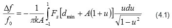
Depending on the operation mode, these forces induce either a quasi-static bending of the cantilever or change its dynamics (frequency, phase, amplitude) when the probe is mechanically driven into oscillation with a piezo-element placed near the fixed end of the probe. For AFM-based electrical studies the probe is typically coated with a metal layer that enables the detection of electrostatic force interactions with the sample. The separation of mechanical and electrostatic forces is essential for reliable measurements of sample electric properties. Below we will demonstrate how this problem is solved in single-pass multi-frequency AFM instrument, which is used for the detection of surface potential and local dielectric response. Additionally, we will introduce a possible approach to quantitative measurements of dielectric permittivity. The approaches used are based on the general description of motion for an oscillating probe subjected to the tip-sample force interactions [1]. The steady state equations for an
oscillating probe are given by the following equations.
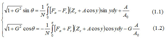
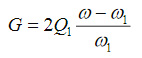
where A and θ are amplitude and phase of the oscillating probe; A0 is the probe amplitude before it interacts with the sample, Fa, Fr – tip-sample forces acting during approach and retraction of the probe to a sample, Zc – vertical coordinate of the sample profile, and G is the parameter related to actual and resonant probe frequencies ω and ω1 and quality factor Q1:
In the case of conservative force interactions (Fa=Fr) the equations are further simplified to:
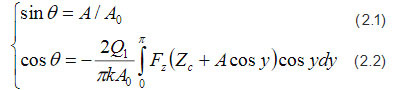
where Fz=Fa= Fr
The above relationships have been successfully applied in the simulation of the probe behavior in different AFM modes and for extraction of quantitative mechanical and dielectric properties from AFM data when the force interactions are represented by reliable models.
DETECTION OF ELECTROSTATIC FORCES IN AFM
The sensitivity of the conducting probe to electrostatic force was demonstrated in the first AFM applications [2]. In this revolutionary work, the 1st flexural mode (ωmech) of the probe resonant oscillation was chosen for tracking the sample topography during non-contact operation. Simultaneously, the electrostatic tip-sample force was stimulated by an AC voltage applied to the probe at a lower non-resonant frequency (ωelec).
The related changes of amplitude at ωelec reflect the variations of the electrostatic force caused by local surface charges, dipoles or regions with different work functions and doping type or level. Therefore, the monitoring and collection of probe responses at two different frequencies allows simultaneous and independent measurements of local electric and mechanical interactions with the latter applied for surface profiling. This principle is applied to single-pass studies of surface potential in KPFM and capacitance gradient dC/dZ (Z – is the vertical distance between the probe and the sample). The detection principle of surface potential and dC/dZ is based on equations describing the tip-sample electrostatic interactions using a capacitor-like model [2]. The quadratic dependence of the force on the difference of surface potentials of the probe and sample gives rise to several force components when external DC and AC voltages – UDC and UAC (the latter at frequency ωelec)
are applied to the probe to promote electrostatic interactions.
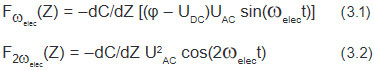
In Eq. 3.1, 𝜑 is the difference between the surface potential of the probe and the sample location beneath the probe. The surface potential difference is determined by finding a specific UDC that nullifies the force at ωelec. This is the task of KPFM servo. The capacitance gradient dC/dZ is directly proportional to the electrostatic force at the 2nd harmonic of ωelec, and it is related to the dielectric permittivity (ε) of the material underneath the probe. For many materials the dielectric permittivity can be a complex value and measurements of real and imaginary components of dC/dZ are essential. Here, we do not consider the dependence of the capacitor on applied voltage, but in a more general case the dC/dV gradient is related to the electrostatic force response at 3ωelec [3]. Therefore, several lock-in amplifiers, which are tuned to ωmech, ωelec, 2ωelec and 3ωelec, can enable simultaneous measurements of topographic and various electric and dielectric properties of samples.
Such a multi-frequency AFM approach has definite advantages when compared to the well-known two-pass method, in which the measurements of the surface topography and local electric properties are performed in separated passes with the conducting probe being retracted from the surface at a lift distance of 10–20 nm [4]. Despite its simplicity, the two-pass method has a number of limitations. They are related to (a) an undesirable “contamination” of the topography images by electrostatic forces acting between the probe and sample, (b) a problem of finding an appropriate lift height to avoid the mechanical interactions during the 2nd pass over corrugated surfaces, (c) a loss of spatial resolution and sensitivity caused by the distant position of the probe in the 2nd pass. The latter limitation does not exist in the single-pass technique because of a closer proximity of the probe to the sample. The comparative advantages of the single-pass operation have been already demonstrated [5-6].
REALIZATION OF KPFM AND DIELECTRIC STUDIES IN THE SINGLE-PASS MODE
Recent developments of AFM electronics, which enable multi-frequency measurements and various oscillatory modes, enhance the researcher’s capability in finding the optimal experimental routine for advanced studies of surface properties. The combinations of amplitude modulation (AM) and frequency modulation (FM) were explored for surface tracking and KPFM mapping in UHV conditions [7, 8]. The most sensitive and accurate surface potential data was obtained using the electrostatic force gradient detection with FM.
These results are consistent with the earlier theoretical estimates [9] that pointed out that in addition to the tip apex, both, the cantilever and the tip body, contribute substantially to the overall electrostatic force exercised by the AFM probe. These contributions are eliminated when the force gradient is measured. Below we will show experimentally that this is true when regular tips of ~10 microns in height are applied. The surface potential data obtained with force and force gradient detections are essentially identical when using conducting probes with extra-long tips (~100 micron in height).
In KPFM studies under ambient conditions we have utilized both force and force gradient for measurements of surface potential and dielectric response. While the probe is driven to mechanical oscillation at ωmech and its electric bias with respect to the sample is changing at ωelec (ωelec≪ωmech), the related frequency components of the photodetector signal can be monitored in parallel with separate lock-in amplifiers (LIA). In this case sample topography will be tracked based on maintaining the set-point amplitude (Asp) with the 1st LIA, which is tuned to ωmech. Simultaneously, the 2nd LIA, which is tuned to ωelec, records the amplitude that is proportional to Fωelec(Z). Furthermore, the servo, which is incorporated in the instrument loop consisting of a probe, photodetector and 2nd LIA, can adjust UDC [Eq. 1] to nullify the force and thus to determine the local surface potential - 𝜑. This operation is often known as KPFM-AM, where AM indicates a detection of the electrostatic force Fωelec. In the parallel connection of two LIA, the tuning of the 2nd LIA to 2ωelec will enable recording of the dC/dZ signal. The amplitude and phase (or real and imaginary components) of this signal are essential for samples with complex dielectric permittivity. When a 3rd LIA is also added in parallel then 2nd and 3rd amplifiers can detect the responses at ωelec and 2ωelec thus enabling the simultaneous recording of sample topography, surface potential, and capacitance gradient.
In an alternative way, Figure 1, the surface potential and dC/dZ can be measured in the LIA configuration employing 2nd and 3rd LIA, which are connected in series with the 1st amplifier. In this case the electrostatic force is stimulated by UAC, which is applied to the probe at low frequency that is within the bandwidth of mechanical probe oscillation at ωmech. A combination of mechanical and electrostatic tip-sample interactions will provide the additive contributions to the phase of the photodetector signal:
θ(t)=θmech+∆θelec(t).
For the best electrostatic performance mechanical forces should be minimized by setting Asp close to A0 (the probe amplitude prior to engagement on the sample). In this case
θmech ≈ p/2 and cosθ(t) ≈ -∆θelec(t).
This means that the frequency components of the phase signal can be applied for measurements of the surface potential and the capacitance gradient.
It is worth noting that the suggested use of phase modulation of the electrostatic force interactions is quite similar to FM because both methods under simplifying assumptions provide the force gradient data.
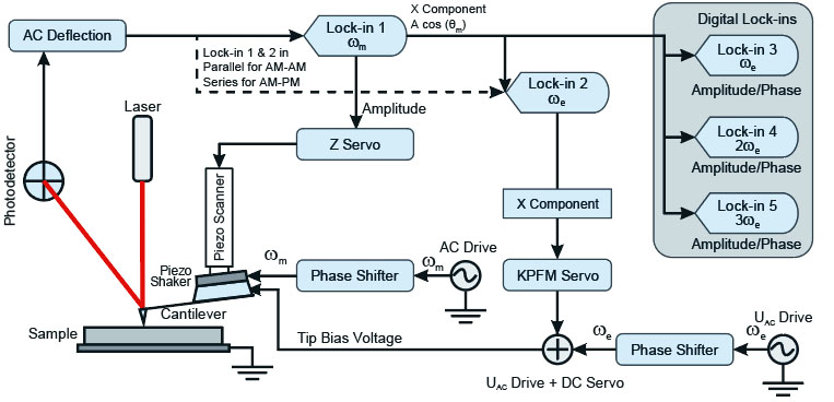
The formalism applied to FM shows that
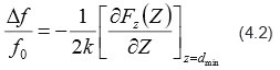
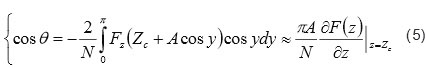
The relationship between the cosine of phase and the tip-sample interaction forces, which was shown above (Eq. 2.1), is valid for the electrostatic forces. Using the approximation of small amplitudes, the cosine of phase is also proportional to the force gradient:
The use of the cosine of phase for KPFM feedback is more precisely connoted KPFM-PM, where PM is the phase modulation by the electrostatic force gradient. In summary, we are using KPFM-AM and KPFM-PM approaches, which are based on the detection of electrostatic force and its gradient, for measurements of surface potential. A similar methodology is applied to measurements of dC/dZ, which can be performed in combination with KPFM or independently. For our practical applications, the most salient point is that the measurements at different frequencies are performed using intermittent contact mode with a relatively small level of mechanical tip-sample interactions. Such experiments conducted on various samples demonstrated that any cross-talk between the topography and local electric measurements is essentially absent [11].
Applications of different KPFM and dC/dZ techniques on various materials are described in next sections. These studies were performed at ambient conditions with an NTEGRA scanning probe microscope equipped with a Universal Head and a next generation P9, improved electronic controller. For multi-frequency measurements it was important that the probe frequency responses could be measured up to 5 MHz. Commercial conducting probes of different manufacturers (Olympus, MikroMasch, and NT‑MDT SI) were utilized in our studies.
APPLICATIONS OF KELVIN PROBE FORCE MICROSCOPY
The use of different signal detection schemes and the development of multi-frequency techniques provide the AFM researcher with a variety of methods for the comparison and examination of the same properties. This is the situation with surface potential and dC/dZ measurements. Therefore, studies of standard samples are invaluable for the verification of different techniques and their applicability. For our KPFM experiments we selected samples of self-assemblies of semifluorinated alkanes on different substrates (Si wafer, mica, and graphite), semiconductor SRAM structures, and a bimetallic alloy of Bi/Sn.
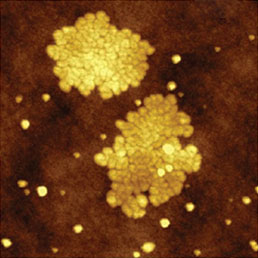
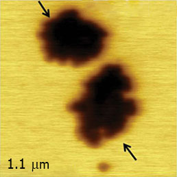
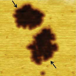
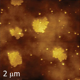
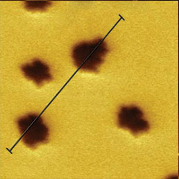
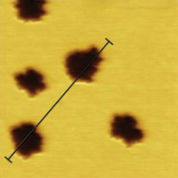
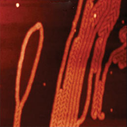
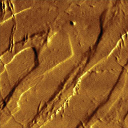
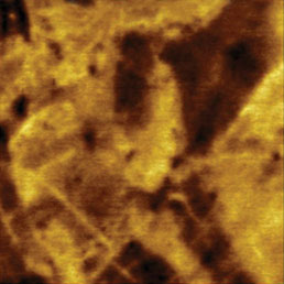
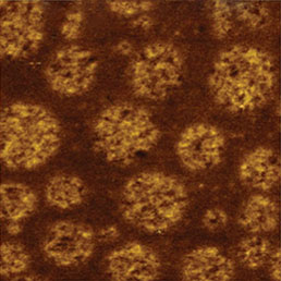
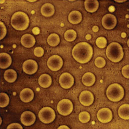
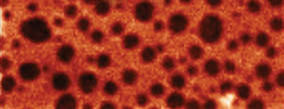
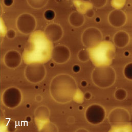
The AFM images, which illustrate the KPFM-PM and dC/dZ measurements of self-assemblies of semifluorinated alkanes CF3(CF2)14(CH2)20CH3 – F14H20 on a Si substrate, are presented in Figure 2.
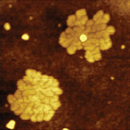
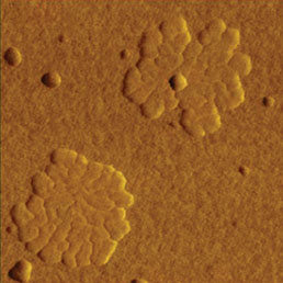
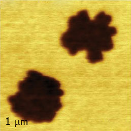
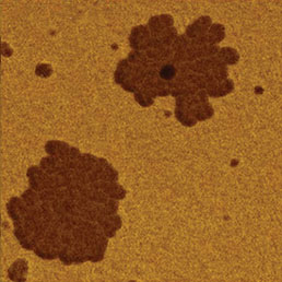
The domains of F14H20 self-assemblies with spiral features that are less than 4 nm in height are seen in the height and phase images. The fact that the phase contrast visualizes only the edges of domains, which are much softer than the substrate, indicates that the measurement was conducted at low force. As mentioned earlier, this is a main requirement of the KPFM-FM measurements. The structure of F14H20 self-assemblies on Si reflect its dissimilar molecular nature, conformation and volume of the fluorinated and hydrogenated parts, which are covalently linked into one chain-like molecule. It is expected that the more bulky fluorinated segments are organized at the exterior of the spirals facing air [12]. This arrangement leads to a preferential vertical orientation of the fluoroalkanes molecules, which have a strong dipole at the central junction -CF2 -CH2-oriented along the chain. Therefore, a strong negative surface potential of the F14H20 domains is expected, which was proven with macroscopic Kevin probe studies of Langmuir-Blodgett layers of the semifluorinated alkanes [13] and in earlier KPFM measurements [5-6]. The negative surface potential is distinctively seen in the surface potential Φ image shown in Figure 2. The negative potential contrast is noticed only at the domains whereas small particles are not visualized in the surface potential image. The lack of small particles in the surface potential data is a strong indication that there is no notice able cross-talk between the mechanical and electrostatic forces in the single-pass operation. The same particles and F14H20 domains are seen in the dielectric response image; this is expected because any material between two electrodes will change the capacitance gradient. A more detailed description of the dielectric response images is given below.
Height
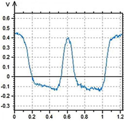
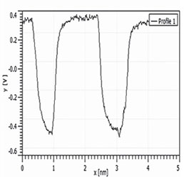
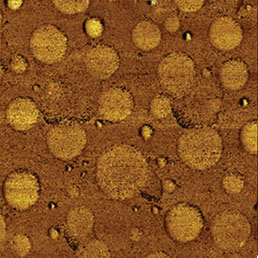
Furthermore, we compare the KPFM-AM and KPFM-PM measurements by analyzing the surface potential images obtained in these modes on the same F14H20 domains on Si substrate, Figure 3. The main difference in comparing the surface potential images collected in KPFM-AM and KPFM-PM modes is the lower values of surface potential (-0.6 V versus -0.8 V) recorded with the electrostatic force detection. The comparison of the surface potential cross-section profiles shows also that the width of the potential change at the domain edge is smaller in the image recorded in KPFM-PM. This parameter is often used as an indicator of lateral resolution, which in our case is better in KPFM-PM. These images were collected with a Pt-coated conducting probe, which has the tip length of 10 microns. As discussed in the introduction, the long-range electrostatic force between the cantilever and the sample contribute to the overall measured electrostatic force in KPFM-AM and causes the lower surface potential value and loss of spatial resolution.
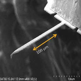
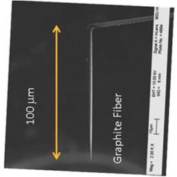
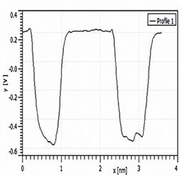
We verified this hypothesis using a novel conducting probe, which is fabricated from a conducting cantilever by attaching a graphite fiber with a chemically etched apex. The length of the graphite tip in such a probe is around 100 microns and, therefore, the electrostatic force between the cantilever and the sample is substantially reduced. Indeed, the KPFM-AM and KPFM-PM measurements obtained with such probes give the identical surface potential ~-0.8 V, Figure 4.
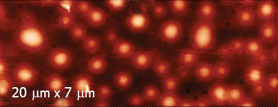
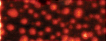
High sensitivity and spatial resolution can be achieved in single-pass KPFM-PM studies as demonstrated in the images of F14H20 self-assemblies on graphite, Figure 5. In contrast to other substrates (Si, mica), with the F14H20 adsorbates on graphite, the first layers are formed of molecules, which are oriented parallel to the substrate and form lamellar structures of 6–8 nm in width. The molecular dipoles in these layers are also preferentially oriented parallel to the surface.
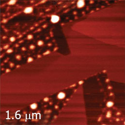
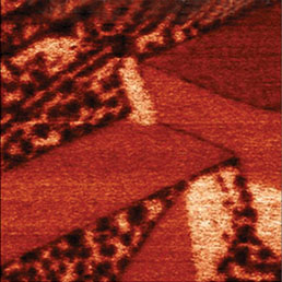
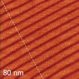
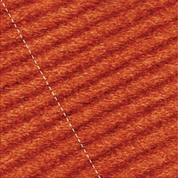
Therefore, the surface potential of these locations will be less strong compared to the F14H20 self-assemblies on Si. The large scale height image shows a number of flat lamellar sheets and numerous droplets dispersed between them. The surface potential contrast of the droplets is moderately negative (around -200 mV), whereas surface potentials of the lamellar sheets and, particularly, of the bare substrate locations are more positive. This is consistent with the expected orientation of the molecular dipoles parallel to the substrate plane. The high-resolution height and surface potential images (80×80 nm scan area) revealed lamellar patterns with height corrugations in the 300 pm range and potential changes in the 10–20 mV range. The spatial resolution of these images, which show the 6-nm spacing, is around a few nm as judged by a width of the dark strips. Additional experimental and theoretical efforts are needed for a complete analysis of this arrangement [14].
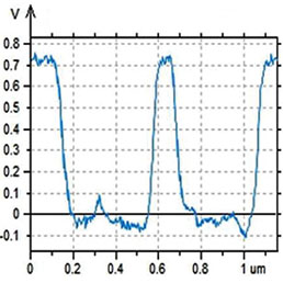
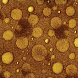
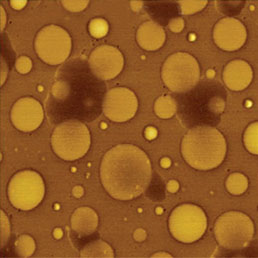
A comparison of the surface potential measurements made using the single-pass KPFM-PM and a double-pass technique was performed with F14H20 assemblies on mica, Figure 6. First, we examined a sample location with single-pass KPFM-PM, and then performed the double-pass studies using positive (+40 nm) and negative heights (-30 nm, -40 nm) with respect to the average position of the probe. The probe was driven into oscillation with a half-amplitude of 50 nm. The surface potential contrast was substantially reduced at the +40 nm lift value and increased when the lift was at -40 nm. This was the lowest lift possible, because attempts to use 50 nm lift led to disturbance of the image, which is seen as a bright strip in the center of the surface potential image in Figure 6.
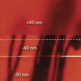
The surface potential difference between the F14H20 self-assemblies and nearby bare substrate regions was approximately -1.4 V in the KPFM-PM image and only around -0.8 V in the double-pass image with a lift of -40 nm. The comparison of the surface potential values obtained using single-pass and double-pass modes shows that the single-pass method is preferred for this type of KPFM study. However, a combination of the negative lift and single-pass methods might be useful and should not be excluded in advanced studies of electric properties, which at the moment are unique features of the NT‑MDT SI scanning probe microscopes.
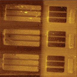
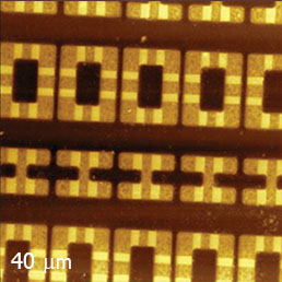
As mentioned earlier, AFM-based electric modes can be used to analyze various materials, and such measurements do not suffer the stiffness-related limitations of local nanomechanical measurement methods. Semiconductor SRAM structures were examined with KPFM-AM at two locations and the representative images are shown in Figure 7.
The surface potential of semiconductor structures depends on type and doping density. Therefore, one should not expect a direct correlation between topography and surface potential images. The surface potential Φ patterns of these semiconductor structures are quite different from the sample topography seen in the height images.
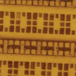
Remarkably, the surface potential images of the large scale SRAM and other semiconductor structures have better stability and resolution when they are imaged using KPFM-AM mode. Subsequently, the optimization of KPFM measurements on different sample types must include both the proper selection of the imaging mode and the probe type. The use of larger tip radius conducting probes is favored for a higher signal-to-noise ratio when measuring local electric properties, and these probes are also preferred because of their higher wear resistance when very high spatial resolution is not required.
Another example of a rigid sample, which can be successfully examined with KPFM is the soldering material, BiSn, Figure 8. A specimen of this incomplete metal alloy can be prepared for AFM studies as a flat sheet by melting the material between two flat substrates. The height, phase and surface potential Φ images of these samples reveal a relatively smooth surface morphology with the domain structures separated by 10–20 nm steps.
The phase image emphasizes the edges of the domains, whereas the surface potential Φ image exhibits a completely different pattern that is uncorrelated with the surface topography. The surface potential variations are in the range of 200 mV, which is consistent with the difference in the work functions of Bi and Sn. The binary contrast in the surface potential images of Bi/Sn alloy might deteriorate with oxidation, which is particularly strong for Sn. Surface oxidation can cause the compositional map to become less pronounced [14]. It is worth noting that KPFM is actually an exception to common AFM techniques in that directly provides quantitative values for a particular sample property. In the case of metals, surface potential is related to the local sample work function, and for molecular systems with dipoles, surface potential correlates to the strength and orientation of molecular dipoles. Kelvin force measurements are also applied for studies of free charges and their behavior caused by various dynamic processes.
However, one should not overestimate the capabilities of KPFM measurements, particularly, when they are performed in ambient conditions. A possible contamination of the sample or the probe might substantially change the validity of absolute values of the surface potential obtained in such studies. Therefore, surface potential differences, which are measured at various locations within a particular scan, are more reliable than the absolute surface potential values.
LOCAL DIELEСTRIC MEASUREMENTS
Dielectric spectroscopy is a well-known characterization technique that is typically used to analyze macroscopic samples. It provides measurements of dielectric properties in a broad frequency range and at various temperatures. It is quite useful to bring dielectric measurements to the micro- and nanoscales, and several efforts were already undertaken in this direction. As shown in Eq. 1, the electrostatic force at 2ωelec is related to dC/dZ, with the latter being a direct result of the local dielectric properties. One of the recent studies of local dielectric properties was performed with an AFM tip on the top of poly(vinyl acetate) film deposited on a conducting substrate [15]. A phase-lock-loop controller was used for the topographic feedback in frequency modulation mode; the electrostatic interactions were stimulated by an AC voltage applied at a much smaller ωelec.
The voltage and phase of the signal at 2ωelec was determined in order to obtain the local dielectric susceptibility. The dependence of real and imaginary components V2ωelec on frequency generally mimics the macroscopic dielectric curves, yet a temperature shift of a few degrees was noticeable between these measurements. The results of the local dielectric measurements at different temperatures also demonstrate the similarity of the frequency responses to those obtained in macroscopic experiments at different temperatures. In addition to measurements of the local dielectric response in one location, the mapping of the dielectric response of thin film made of PS and PVAC blend was performed at different temperatures [16]. Specifically, it was shown that the domains of PVAC are identified by strong phase contrast that appears near the glass transition temperature of this polymer. The matrix, which is presumably enriched in PS, does not change its contrast because the glass transition of PS is much higher.
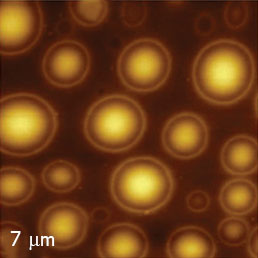
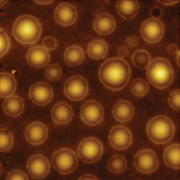
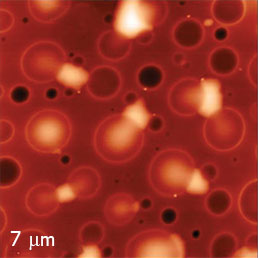
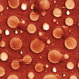
It is worth noting that the aforementioned studies were conducted in UHV (ultra high vacuum) in non-contact mode. We have selected the same material – PS/PVAC blend as the test sample for single-pass studies under ambient conditions. Typical images of the thin film of this blend on a conducting ITO substrate are shown in the left part of Figure 9.
The film morphology is characterized by spherical domains imbedded into the matrix and it is consistent with immiscible nature of this blend which leads to phase separation of the constituents.
The surface potential Φ of the domains is higher (~200 mV) than the matrix’s potential and this difference correlates with the fact that dipole moments of the polymer molecules are quite different (PS – 0.3 D, PVAC – 2.1 D). For dielectric measurements we applied the same scheme as described in Figure 1 but the 2nd LIA was tuned to 2ωelec.
Height
Amp Cosθ
RS-PVAC Map
RS-PS Map
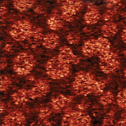
In phase modulation experiments typical values for ωelec predominantly in the 3–5 kHz range. In most dielectric studies we detect the amplitude and phase signals of cosθ at 2ωelec, an amplitude image is shown for PS/PVAC film. The analysis of this image, which is substantially different from the surface potential Φ image, is quite complicated. At first glance, one can notice that the pattern generally resembles the reversed topography profile of this film.
Studies of the PS/PVAC morphology behavior at different temperatures, in methanol vapor [14] as well as previous dielectric measurements [16] suggest that the domains are enriched in PVAC whereas the matrix is predominantly PS. This suggestion is strongly supported by confocal AFM-Raman studies.
The Raman spectra of the individual polymer components show that the most pronounced bands of PS (~1018 cm-1) and PVAC (~2959 cm-1) are located in different parts of the vibrational spectra. Therefore, these bands can be used for identification of these components in the blend. The height image of one location of a PS/PVAC film is shown together with the maps of intensity of the strongest PVAC and PS bands. This data unambiguously supports the assignment of spherical domains to PVAC and the matrix to PS.
Annealing of PS/PVAC at temperatures above glass transition of PVAC (~40 °C) and below glass transition of PS (~100 °C) induces morphology changes, which most likely reflect the flow of PVAC polymers from elevated domains to nearby surface regions. This leads to the formation of the elevated patches in between the spherical domains enriched in PVAC. The surface potential Φ confirms that the elevated patches are of the same nature as the spherical domains. The contrast of the dielectric response is quite different with the related pattern exhibiting the most pronounced features at the spherical depressions. Again, the map of the amplitude of cosine θ at 2ωelec mimics the reverse topography profile (Figure 10).
Similar to the surface potential, the dielectric response can be obtained in different ways. A comparison of the images related to local dielectric permittivity, which were obtained at the annealed PS/PVAC film is given in Figure 11. In the PM approach the amplitude of cosine θ was measured at 2ωelec=6 kHz.
The dC/dZ measurements were also performed in the AM mode at the non-resonant frequency of 2ωelec=6 kHz and the frequency that is half of the 2nd Eigen mode of the probe (405 kHz). This mechanical resonance method has definitely improved the signal-to-noise performance and the image contrast is the best compared to two other images using different methods to measure the local dielectric response.
non-resonant
resonant
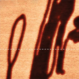
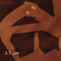
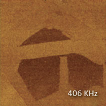
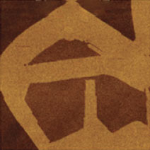
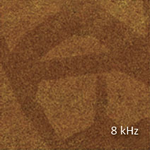
The next example is taken from the studies of semifluorinated assemblies on mica, Figure 12. The assemblies form arrays of ribbons, whose arrangement exhibits an epitaxial order. The surface potential image shows the negative contrast that indicates a vertical alignment of the fluoroalkanes chains.
Two nanocrystals, which are seen elevated at the top of the height image, do not exhibit the negative potential and that implies a lateral orientation of the molecules in these structures.
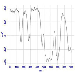
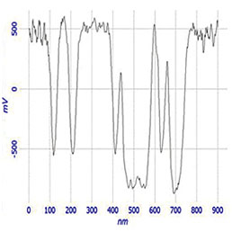
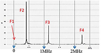
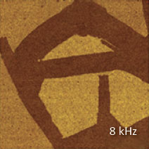
The local dielectric response was measured at different frequencies. The dC/dZ and cosine θ responses were measured at the non-resonant low frequency 2ωelec=8 kHz. For measurements at higher frequencies, we have applied two resonant frequencies: 2nd Eigen mode (406 kHz) and 3rd Eigen mode (1.14 MHz). These and other resonances are seen in the amplitude-versus-frequency spectrum of the chosen probe. The electrostatic force was stimulated at half of the 2nd and 3rd flexural (Eigen) modes such that the dC/dZ response at 2ωelec was emphasized by its correlation to the resonances. The results from these local dielectric studies showed that the contrast of the cosine amplitude is more pronounced than the dC/dZ amplitude at the same frequency (8 kHz).
The noticeable differences amongst the dC/dZ phase images at different frequencies (8 kHz, 406 kHz and 1.14 MHz) indicate the influence of the molecular motions of the fluoroalkanes on the measured dielectric response of this material.
The dielectric spectroscopy data obtained on similar materials revealed strong β-relaxation related to rotation of -(CF2)n- group in the alkanes [17].
The quantitative analysis of the dielectric response is more complicated than in the case of surface potential, which is directly measured in KPFM studies. Nanoscale capacitance of a thin dielectric film depends on the ratio of film thickness and dielectric permittivity [18].
Therefore, the topography-related contribution complicates the images containing local dielectric properties, and this effect should be considered in the analysis. The other problem is related to the existing methods for dielectric studies. High-contrast images related to local dielectric properties were obtained using the response at the 2nd flexural mode.
This data is more difficult to treat theoretically because the signal is enhanced through the cantilever resonance and its Q-factor should be taken into account. A situation with the analysis of the cos2ωelec (amplitude & phase) signal is more straightforward.
According to the theoretical description of the probe motion in oscillatory AFM mode there is a general relationship between the cosine phase and the force acting on a probe. This equation can be applied for electrostatic tip-sample force interactions and the related integral is calculated analytically [19]. As a result, one gets the relationship between amplitude of phase cosine (  ), the capacitance of the tip-sample junction [18], the probe features, and a ratio of sample thickness to permittivity
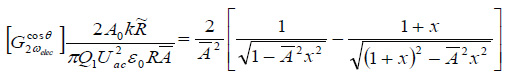
where ε0 – the vacuum dielectric constant, εr - the relative dielectric constant of the film; Q1 – quality factor, h is the thickness of the film, Zc is the apex-film separation distance; θ0 – tip cone angle, R - the effective apex radius;  , A and A0 – actual and free amplitudes
This relationship can be applied for extraction of quantitative permittivity values from the experimentally
measured cosine phase, the capacitance and the probe parameters. We have used this approach to get quantitative data for two polymer films using a LabView-based program that incorporates the above formulas [18].
A verification of the quantitative dielectric measurements was performed on thin, homogeneous PS and PVAC films, which were prepared by spin-casting solutions of the pure polymers in toluene on conducting ITO glass substrate. A sharp wooden stick was used to scratch through the films so that the imaging of the polymer film thickness becomes possible.
The morphology from one location of the PS film on ITO glass is shown in Figure 13. Simultaneously with height images, the cosine phase response on the polymer film and substrate was detected at different stimulating AC voltages. A quadratic dependence of the amplitude versus voltage is observed.
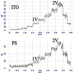
The calculations of the dielectric permittivity were made for measurements performed at stimulating AC voltage of 1V (ωelec=4 kHz) with probes having different tip radii. The results, which are summarized in the Table 1, show that at this frequency the permittivity of PVAC is ~1.4 times higher than that of PS and the absolute values are close to those determined in macroscopic measurements. The local dielectric measurements of these and other polymer films at elevated temperatures and different frequencies are in progress.
| Tip, R=15 nm | R=30 nm | |||||
| Amplitude | 19 nm | 18 nm | 48 nm | 19 nm | 38 nm | 76 nm |
| ε (PS) | 1,13 | 1,33 | 1,71 | 1,65 | 1,67 | 1,68 |
| ε (PVAC) | 1,80 | 1,90 | 2,18 | 2,36 | 2,25 | 2,30 |
|
εPS/εPVAC |
1,59 | 1,43 | 1,27 | 1,43 | 1,35 | 1,37 |
CONCLUSIONS
The development of AFM-based electric modes based on multi-frequency measurements and novel force detection schemes leads to more sensitive and higher-resolution KPFM and local dielectric studies. These advances improve compositional mapping of multi-components samples, which is demonstrated on various materials. In addition to compositional mapping, the quantitative measurements of surface potential and dielectric permittivity are of increasing interest. A novel approach for the extraction of permittivity values of thin polymer films from AFM measurements was introduced; however, it needs validation on more complex materials. Further advances in local dielectric measurements are tied to the expansion of electrostatic force studies to broad temperature and frequency ranges.
REFERENCES
[1] S. Belikov, and S. Magonov “Classification of Dynamic Atomic Force Microscopy Control Modes Based on Asymptotic Nonlinear Mechanics” Proceedings American Control Society, St. Louis, 979-985, 2009.
[2] Y. Martin, D. A. Abraham, and H. K. Wickramasinghe “High-resolution capacitance measurement and potentiometry by force microscopy” Appl. Phys. Lett. 1988, 52, 1103–10005.
[3] K. Kobayashi, H. Yamada, K. Matsushige, “Dopant profiling on semiconducting sample by scanning capacitance force microscopy” Appl. Phys. Lett. 2002, 81, 2629.
[4] V. B. Elings, and J. A. Gurley “Scanning probe microscope using stored data for vertical probe positioning” US Patent 5,308,974, 1994.
[5] J. Alexander, S. Magonov, and M. Moeller “Topography and surface potential in Kelvin forcemicroscopy of perfluoroalkyl alkanes self-assemblies” J. Vac. Sci. Technol. B 2009, 27, 903–911.
[6] S. Magonov, and J. Alexander “Single-pass Kelvin force microscopy and dC/dZ measurements in the intermittent contact: applications to polymer materials” Beilstein J. Nanotechnol.2011, 2, 15-27.
[7] U. Zerweck, CH. Loppacher, T. Otto, S. Grafstroem, and L. M. Eng “Accuracy and resolution limits of Kelvin probe force microscopy” Phys. Rev. B 2005, 71, 125424.
[8] F. Krok, K. Sajewicz, J. Konior, M. Goryl, P. Piatkowski, and M. Szymonski “Lateral resolution and potential sensitivity in Kelvin probe force microscopy: Towards understanding of the sub-nanometer resolution” Phys. Rev. B 2008, 77, 235427–235429.
[9] J. Colchero, A. Gil, and A. M. Baro “Resolution enhancement and improved data interpretation in electrostatic force microscopy” Phys. Rev. B 2001, 64, 245403.
[10] F. Giessibl “Forces and frequency shifts in atomic-resolution dynamic-force microscopy” Phys. Rev. B1997, 56, 16010-16015.
[11] S. Magonov, J. Alexander, S.-H. Jeoung, and N. Kotov “High-resolution imaging of molecular and nanoparticles self-assemblies with Kelvin force microscopy” J. Nanosci. Nanotechnol.2010, 10, 1-5.
[12] A. Mourran, A.; Tartsch, B.; Gallyamov, M.; Magonov, S.; Lambreva, D.; Ostrovskii, B. I.; Dolbnya, I. P.; de Jeu, W. H.; M. Moeller, “Self-assembly of the perfluoroalkyl-alkane F14H20 in ultrathin films”. Langmuir2005, 21, 2308–2316.
[13] A. El Abed, M-C. Faure, E. Pouzet, and O. Abilon “Experimental evidence for an original two-dimensional phase structure: An antiparallel semifluorinated monolayer at the air-water interface” Phys. Rev. E 2002, 5, 051603–051604.
[14] S. Magonov, J. Alexander, and S. Wu “Advancing characterization of materials with Atomic Force Microscopy – based electric techniques. In Scanning Probe Microscopy of Functional Materials: NanoscaleImaging and Spectroscopy; Kalinin, S. V.; Gruverman, A., Eds.; Springer: Berlin, Germany, 2010; pp 233–300.
[15] P. S. Crider, M. R. Majewski, J. Zhang, H. Oukris, and N. E. Israeloff “Local dielectric spectroscopy of near-surface glassy polymer dynamics” 2008, 128, 044908-5.
[16] C. Riedel,R. Arinero, Ph. Tordjeman,G. Lévêque, G. A. Schwartz, A. Alegria, and J. Colmenero“Nanodielectric
mapping of a model polystyrene-poly(vinyl acetate) blend by electrostatic force microscopy”Phys. Rev. E2010, 81, 010801-010804.
[17] K. Araki, K. Satoh, and S. Kondo “Dielectric behavior of semifluorinated n-alkane (F(CF2)n(CH2)mH)” Mol. Cryst. Liq. Cryst.1996, 281, 123-134.
[18] G. Gomila, J. Toset, and L. Fumagali, “Nanoscale capacitance microscopy of thin dielectric films” J. Appl. Phys.2008, 104, pp. 024315 1-8.
[19]. S. Belikov, J. Alexander, S. Magonov, and I. Yermolenko “Atomic force microscopy control system for electrostatic measurements based on mechanical and electrical modulation” Amer. Control Conf.2012, 3238-3233.