Applications
Ultrathin films: Oligothiophene monolayers on Silicon
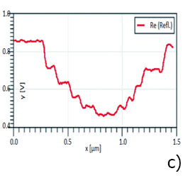
IR reflection contrast of thin and soft structures easily detectable. Each of five 3.4 nm steps is resolved. Spatial resolution is better than λ/1000.
Topography (left), reflection for λ=10.6 μm (center) and cross section of reflection signal (right).
Sample courtesy to Dr. A. Mourran (DWI, Aachen, Germany). Measured by Dr. G. Andreev (EVS Co)
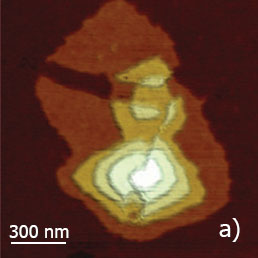
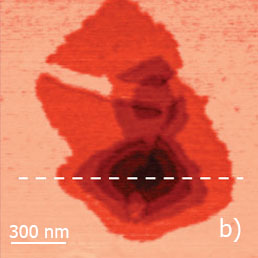
Phase transition behavior of VO2 film
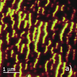
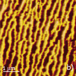
Vanadium dioxide is a natural disordered metamaterial. VO2 film grown on a TiO2 substrate comprises nanoscale islands of metal- and dielectric-phase. Under the heating VO2 film demonstrates phase insulator to metal transition. Same area was measured by s‑SNOM at different temperatures. Bright areas show conductive domains and dark areas correspond to dielectric domains. Above critical temperature conductive domains become connected to each other and VO2 film demonstrates conducting properties in macroscale. Due to essential parts of the AFM are made of Ti the instrument demonstrates high stability at temperatures up to 100 0C exhibits extremely low drift: <1 um XY drift for temperature changes from 27 0C to 67 0C. No realignment of NTEGRA Nano IR optics needed.
s‑SNOM reflection of VO2 at 55 C (left) and at 67 °C (right). λ=10.6 μm. Sample courtesy to prof. Liu (Stony Brook University, New York, USA)
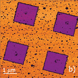
Si-SiO2 calibration grating
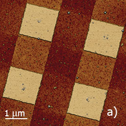
Another example is a grating in which the square-shaped SiO2 pads with lateral dimensions 1.5x1.5 µm and height of ~20 nm are grown on Si surface. The square blocks are well distinguished in IR images by a darker contrast compared to the Si substrate. This contrast reflects the differences between the real components (ε΄) of dielectric permittivity of these materials at 10.6 μm wavelength. The darker contrast of SiO2 pads in s‑SNOM map is consistent with lower value of its permittivity (εr=3.9) compared to that of Si (εr=11.7).
Height (left), s‑SNOM amplitude (right) of Si/SiO2 grating
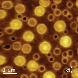
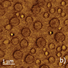
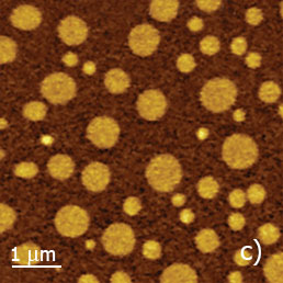
PS/PVAC film on the conducting ITO substrate
The height image of PS/PVAC film on the ITO substrate shows the morphology in which the circular domains of different height are embedded into a relatively flat matrix. Only small contrast changes are noticed on the domains and matrix locations whereas the domains’ edges are seen most pronounced.
The situation is quite different in IR nano-adsorption image in which the high contrast of the circular domains allows their assignment to PVAC - the polymer that has adsorption band near 10.6 μm. These data demonstrate that the spatial resolution of IR reflection and absorption mapping is well beyond the diffraction limit of the applied IR light.
Height (left), reflection (center) and absorption (right) images of a PS/PVAC film on ITO substrate
Thermoplastic vulcanizate (TPV)
Thermoplastic vulcanizate (TPV) is a nanocomposite which is made of a blend of isotactic polypropylene and EPDM rubber that are mixed with carbon black particles. Such samples exhibit shiny black surface and, therefore, they are burned in Raman studies. The AFM/IR measurements of this sample are not only possible but they are very successful.
A number of bright nanoparticles seen in a central part of the height image can be assigned to carbon black fillers. The suggestion is strongly supported by the IR reflection image in which the carbon nanoparticles show extremely bright contrast compared to the polymer matrix.
Height (left) and IR reflection (right) images of TPV sample
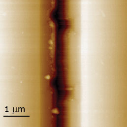
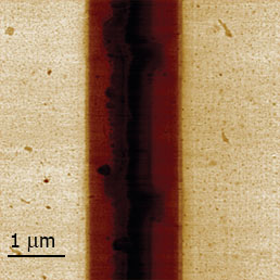
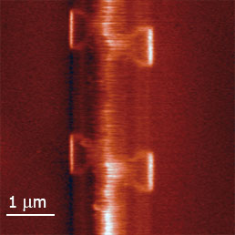
Si microstructure with p-doping areas
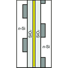 Sample scheme
 Topography
 s‑SNOM Amplitude
 s‑SNOM Phase
In this sample, the strips of p-doping (p~1020 cm-3) were formed on a Si wafer by a BF2 ion implantation of the substrate surface. To investigate the sample in a cleaved-surface geometry, two strips of a diced sample were glues together before their final polishing. An epoxy which fills the slit between the pieces prevents the tip from being broken by a sample edge.
Such a sample was scanned with an s‑SNOM at a wavelength of 10.6 μm.
s‑SNOM images clearly demonstrate a contrast between doped and undoped areas of Si. In most, such a contrast is caused by difference in a free carrier concentration in heavily doped and slightly doped Si. Real part (ε΄) of a sample dielectric function is determined mainly by the value εSi=11.7. Without doping, εSi is purely real at CO2 laser wavelengths, because no absorption is known for undoped Si at a wavelength of 1-200 μm. In a doped Si sample, plasma of free carriers adds an imaginary part to εSi dielectric function at light frequency, modifying mainly a phase of εSi complex value.