Large-sample Atomic Force Microscope VEGA | NT-MDT SI
+1-480-493-0093

VEGA


Cutting-edge Atomic Force Microscopy techniques for large and multiple samples

Cutting-edge Atomic Force Microscopy techniques for large and multiple samples

Brochure

  • Industry leading automation level
  • Outstanding noise floor and thermal drifts
  • Fast scanner with XYZ low-noise close-loop
  • Routine atomic resolution
  • 60+ SPM modes in basic configuration
  • Continuous zoom from millimeter to nanometer range
  • Integrated with new Atomic Force Microscopy technique HybriD Mode™

General information

Ultimate imaging quality with build-in acoustic and vibration isolation, active thermostabilization, industry lowest 25 fm/√Hz optical beam deflection sensor noise and unique design of scanning-by-tip system allow routine high resolution imaging.

Equipped with 50+ AFM modes including HybriD mode: all cutting-edge nanomechanical, electrical and magnetic studies are available in basic configuration.

Automated study of samples arrays by user-defined scenario with database image storage.

Up to 200×200 mm and 40 mm in height samples inspection in any point with 1 μm positioning accuracy.

Smart ScanT™ software for one-click optimization of scanning parameters. This is not just an algorithm, it is rather a unique companion that helps a newcomers in AFM to get industry quality images and assists the experts.

Wide possibilities of customization: integration of addition optical equipment, OEM sample holders, automation of measurement and data analysis procedures according to your requirements.

Performance

Automated inspection of large samples and samples arrays with ultimate positioning precision

VEGA is the first AFM that brings industry standard automation to all users:

  • All routine procedures like area of interest exchange, laser alignment, gentle approach and scanning parameters tuning are fully automated.
  • Motorized sample positioning stage is correlated with optical image allowing 1 um positioning accuracy on 200×200 mm area.
  • Prolongated serial measurements of large and multiple samples became easy and time-effective thanks to smart algorithms, user interface for multiple AFM measurements and database image storage.


Perfect environment for high-resolution measurements

High-resolution measurements require exceptional level of acoustic and vibration isolation of AFM working environment. Build-in acoustic enclosure and active anti-vibration system makes VEGA perfect for demanding AFM studies.

Thermal drift is a challenging issue for high-resolution and long-term measurements especially for largesample AFMs with massive mechanical parts. Unique design of build-in fan-free enclosure provides VEGA with capability to operate at conditions of extraordinary temperature stability within 0.05 oC. This guarantees the exceptional low thermal drift of less than 0.2 nm/min.

Ultimate resolution

HOPG atomic resolution, 6×6 nm

Our unique 100x100 um closed-loop scanner and control electronics design allow atomic resolution and less than 30 pm topography measurement noise.

850 nm non-coherent superluminescent diode (SLD) source and special optical scheme design assures the lowest 25 fm/√HZ OBD sensor noise among commercial large-sample AFMs.

Customizing

OEM sample holders

VEGA mechanical design allows fast exchange and three-point mount of sample holder. Upon your request we can develop unique:

  • vacuum wafer chucks;
  • multiple sample holders;
  • holders with sample temperature control option;
  • etc.

Additional optical equipment:

  • optical microscope with up to 250 nm resolution;
  • raman spectroscopy;
  • ellipsometry;
  • etc.

This equipment can be integrated and correlated with AFM probe position thanks to 1 μm sample XY-positioning accuracy.

Automation of measurement and data analysis procedures

Our software engineers can develop unique automation algorithms according to your requirements.

Most advanced set of AFM modes in basic configuration

HybriD (HD) mode:

  • Quantitative Nanomechanical Measurements (QNM) – mapping of Young’s modulus and work of adhesion values
  • Fast Force Volume – recording of force-distance curves for each scanning point
  • HD Conductive Probe AFM (HD CP-AFM) – non-destructive conductive measurements
  • HD Piezoresponse Force Microscopy (HD PFM) – non-destructive piezoresponse measurements
  • HD KPFM, HD SCM, HD EFM – single- and multifrequency electrostatic studies
  • HD MFM – magnetic studies
Self-assembled diphenylalanine peptide nanotubes: simultaneous topography, adhesion, d2C/dZ2 and in-plane piezoresponse phase (direction of polarization) measurements obtained by HD mode, 8x8 μm

Tin-Bismuth alloy. (a) Topography, (b) Elastic Modulus, (c) Surface Potential
HD PFM study of real-time temperature dynamic of TGS crystal near Curie point. Topography is overlayed by out-of-plane piezoresponse.
Scan size is 15×15 μm

High-resolution Magnetic Force Microscopy (MFM)

Better than 30 nm MFM spatial resolution, ultimate signal-to-noise ratio and 200×200 mm XY motorized stage makes VEGA a perfect tool for data storage inspection.


HDD servo sector. Scan size is 10x6 μm

Multi-frequency electrical studies:

  • Single- and two-pass Amplitude and Phase Modulation Kelvin Probe Force Microscopy (KPFM)
  • Single- and two-pass Amplitude and Phase Modulation Scanning Capacitive Force Microscopy (SCFM)
  • Single- and two-pass Amplitude and Frequency Modulation Electrostatic Force Microscopy (EFM)
Topography, Surface Potential and dC/dZ of self-assembled F14H20 on Si, 1.5x1.5 µm

Full list of AFM modes avaliable in basic configuration:

Contact AFM: Topography, Lateral Force, Force Modulation, Spreading Resistance Imaging

Amplitude modulation AFM: Topography, Phase, Feedback

HybriD mode AFM: Topography, Young’s modulus, Work of Adhesion, Viscoelectisity, Current, Piezoresponse Force Microscopy, Fast Force Volume

AFM spectroscopy: Force-distance, Amplitude-distance, Phase-distance, I(V), I(Z)

Magnetic Force Microscopy: Two-pass and Frame Lift DC/AC

Electrostatic Force Microscopy: Single-pass and Two-pass Amplitude Modulation, Frequency Modulation

Scanning Capacitance Force Microscopy: Single-pass and Two-pass Amplitude Modulation, Frequency Modulation (dC/dZ and dC/dV imaging)

Kelvin Probe Force Microscopy: Single-pass and Two-pass Amplitude Modulation, Phase Modulation

Piezoresponse force microscopy & Switching Spectroscopy

Nanolithography: Voltage, Current, Force

Applications


200x200 mm XY motorized stage together with low-noise scanningby-tip system and variety of nique NT‑MDT SI AFM cantilevers allow failure and roughness analysis of large and heavyweight amples with 30 pm vertical esolution. This feature is now available for users of any skills thanks to automated scanning parameters adjustment.


Conventional AFM probe with 3:1 aspect ratio (left) and NT‑MDT SI whisker-type probe with >10:1 aspect ratio (right)


Topography of microchip,
Scan size is 70×46 μm

PS-b-PMMA,
Scan size is 2.5x1.6 μm

Polycrystalline silicon,
Scan size is 1x0.6 μm

Black silicon,
Scan size is 40x26 μm

Advanced studies in a field of microelectronics, MEMS and data storage


Magnetic domains of high-density HDD. Scan size is 4x4 μm

Surface potential of SRAM
Scan size is 40x40 μm

Powerful set of surface characterization modes like Kelvin Probe, Magnetic Force, Piezoresponse Force microscopy, Capacity and Conductivity mapping makes VEGA AFM irreplaceable tool for research and control applications in a field of modern micro- and nanoelectronics, MEMS, NEMS and data storage.

Customizable easy-to-exchange sample holders allow variety of applications including wafer inspection, multiple samples study etc.

Routine multiple AFM measurements

Mechanical design and control software of VEGA AFM was developed to make frequent AFM measurements easy and time-effective. Fully automated operation, user interface for serial AFM measurements, database image storage and customizable sample holder allow to setup and simply investigate any array of samples.


DNA plasmids, on MICA. Scan size is 2x2 μm

Nitrocellulose membrane. Scan size is 30x30 μm

Multiple sample holder

Specifications

Measuring heads

Standard AFM head for traditional AFM probes. Enables operation with the majority of commercial probes

Scanner

Type: tube scanner with closed loop sensors. Scanning by tip

Scanning range, XYZ: 100×100×10 µm or 2×2×1 µm in Low Voltage Mode

Closed loop: Available for all Directions: XYZ

Drive electronics noise <5 µV/√Hz

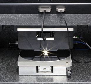
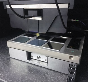
Tip-Sample Positioning

Type: motorized sample positioning in XYZ

XYZ thermal drift: Less than 0.2 nm/min

Moving range: 200×200 mm in XY, 30 mm in Z

Positioning accuracy: 1 µm in XY, 0.2 µm in Z

Positioning speed: 8 mm/sec in XY

Navigation: automated multiple scanning by user-defined scenario, by video image, 3D mouse compatible

Approach: smart soft approach algorithm

Optical Sensor

Light source: 850 nm SLD with FC single mode fiber, optional LDM and SLD sources of different wavelengths

Optical system adjustment: automated

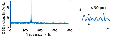
Optical beam deflection sensor noise: <25 fm/√Hz above 50 kHz

Optical Microscope

Type: motorized focus, digital zoom and XY positioning. Correlated with sample and laser position

Resolution: 0,98 μm

Field of view: up to 1.2×0.8 mm (5 Mpixel)

Autofocus: on cantilever, on sample

Accessories

Variety of sample holders

150 V bias voltage extension

Signal Access Module

AFM probes: probe holder supports most commercially available probes

Electronics & Software

Number of scan channels: up to 24

Signal processing: 512 Mb buffer Size, 3x 340 MHz FPGA, 320 MHz DSP

Lock-in amplifiers: 2x analog lock-in amplifiers, 3x digital lock-in amplifiers (Multifrequency AFM modes supporting)

Generators: 6x 32 bit digital generators, 4x for Lock-in

BV: +/- 10 V AC and DC (independent sample and tip voltage supply), +/- 150 V AC and DC (optional)

Self-testing: automated performance check

Scanning parameters auto adjustment: drive amplitude, lock-in gain, setpoint, feedback gain, scanning rate

Automatic configuration of advanced modes

Automation Features: optical system adjustment, multiple scanning on 200×200 mm range by user-defined scenario, overlay of optical and AFM images, panoramic optical view, place of interest saving, autofocus on cantilever, autofocus on sample

Programming tools: Nova PowerScript language, LabView integration, Database integration

Database storage of obtained images

PC interface: USB

Environmental Protection

Temperature stabilization: build-in fan free thermal stabilization with 0.05 °C accuracy

Acoustic isolation: build-in acoustic enclosure

Vibration isolation: build-in active vibration isolation table

Basic Set of Modes

Contact mode: Topography, Lateral Force, Force modulation, Spreading Resistance, Piezoresponse Force Microscopy, Contact Resonance Microscopy

Amplitude modulation mode: Topography, Phase Imaging, Single- and Two-pass Kelvin Probe Force Microscopy with Phase and Amplitude Modulation, Two-pass and Frame Lift Magnetic Force Microscopy, Single- and Two-pass Electrostatic Force Microscopy, Single- and Two-pass Scanning Capacitance Force Microscopy (dC/dZ and dC/dV imaging)

HybriD mode: Topography,Young's modulus QNM for 104 to 1011 Pa, Work of Adhesion QNM, Force Volume, Current, Piezoresponse, Viscoelasticity, Kelvin Probe Force Microscopy with Phase and Amplitude Modulation, Magnetic Force Microscopy, Electrostatic Force Microscopy, Scanning Capacitance Force Microscopy (dC/dZ and dC/dV imaging)

Nanolithography: Voltage, Current, Force (All Vector and Raster)

Spectroscopy: Force-, Amplitude-, Phase-, Frequency-, Current-Distance, I(V), Piezopulse, Custom mode
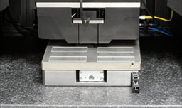
Dimensions:

W×L×H: 810×610×1450 mm

Contact Us

Fulfill a special form to request additional information.

Get more information