


Piezoresponse Force Microscopy in Its Applications
Application Note 083 (pdf 11.1 Mb)
- Ferroelectric domains imaging
- Hysteresis loops measurements
- Local ferroelectric behavior investigation
This application note gives a brief description of the Piezoresponse Force Microscopy methods and its implementation in NEXT scanning probe microscope. The capabilities of PFM studies with this device are illustrated by selected examples of imaging and spectroscopy studies on several piezoelectric and ferroelectric samples. They include lead zirconate titanate - PZT and bismuth ferrite - BFO films, ceramic samples of lead zirconate titanate doped with lanthanum - PLZT, parallel polarized lithium niobate - PPLN, crystals of triglycine sulphate - TGS.
INTRODUCTION
One of the remarkable features of Atomic Force Microscopy (AFM) – is the capability of performing studies of mechanical and electric properties
at the small scale. In local electric measurements the conducting AFM probe is placed at or near a sample surface and it serves as an electrode that is sensing an electrostatic force, current, capacitance or a displacement of the sample in response to the external electric excitation. In one of such operations a specimen as a thin film or a block sample is placed between a contacting probe and a bottom electrode can undergo the piezo-electric testing. Some crystalline materials, whose structure lacks a central symmetry, exhibit the ferroelectric behavior by changing their dimensions in response to the applied electric field or vice versa. This property is employed in functional structures and devices for optoelectronics, different actuators, data storage, medical diagnostics, etc. The establishment of the structure-property relationship in these materials requires the comprehensive characterization of their electromechanical behavior at macroscopic and microscopic dimensions. One of AFM offsprings - Piezoresponse Force Microscopy (PFM) [1-4] is based on sensing of a tiny displacement of the samples caused by electric field excitation. A microfabricated probe with the tip dimensions in the nanometer scale is employed for this detection that can be performed with unique spatial resolution.
PFM, which is applied on the scale from a hundred of microns down to nanometers, can be used in different environments and at various temperatures. The method allows exploring the electromechanical performance of ferroelectrics and piezo-electrics in terms of their domain morphology and dynamic characteristics of hysteresis loops and switching of polarization. Prior to PFM, the characterization of ferroelectric samples with optical and electron microscopy required the use of special preparation techniques such as etching and decoration. These efforts are not needed for PFM studies. This application note gives a brief description of the method and its implementation in NEXT scanning probe microscope. The capabilities of PFM studies with this device are illustrated by selected examples of imaging and spectroscopy studies on several piezoelectric and ferroelectric samples. They include lead zirconate titanate - PZT and bismuth ferrite - BFO films, ceramic samples of lead zirconate titanate doped with lanthanum – PLZT, parallel polarized lithium niobate - PPLN, crystals of triglycine sulphate - TGS.
THEORETICAL OUTLOOK
In general case, the strain Sj developed in a piezoelectric material by the applied electric field Ei is described by the following matrix equation [5]:
Sj = dijEi
where dij is the piezoelectric coefficient or modulus with the unit of m/V. The indices 1–3 indicate components along the x, y, and z axis of an orthogonal coordinate system, and indices 4–6 indicate shear components of the strain tensor. The axes of the coordinate system are often chosen along the crystallographic axes of a crystal. In the case of ceramics and thin films, the z axis is usually aligned with the direction of the polarization, which is normal to the film plane. The longitudinal piezoelectric constant, d33, can be determined by measuring the displacement (Δz) of the sample along the applied field (E3):
Δz = d33V
assuming  and
and  where V is the applied voltage and z0 is thickness of the sample. The sample expands or contracts, if the polarization direction is respectively parallel or antiparallel to the applied field. Due to small dimensional changes (i.e. a vertical displacement of a 1-μm thick PZT film, which has the piezo modulus d33 = 3,6E-10 m/V is below 1 nm) their detection is facilitated by AC measurements. For this purpose,
V = VAC cos(wt)
voltage is applied to the tip and the cantilever displacements are expressed as follows
Δz = d33VAC cos(wt + Q)
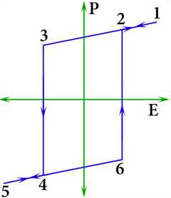
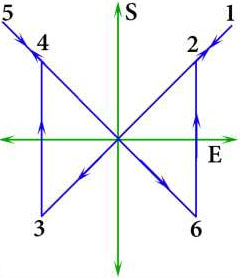
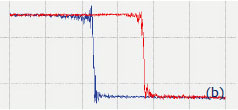
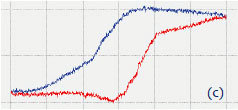
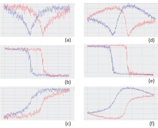
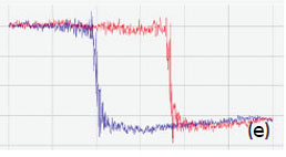
When Q = 0, polarization points down, and when Q = p, polarization points up. The piezo-response will oscillate in-phase or out-off phase if the polarization is, respectively, parallel or antiparallel to the field. Because of the presence of non-zero transverse piezoelectric constants, e.g., d15, and the possible misalignment of polarization to the applied field due to a random crystal orientation, an electric field normal to the surface can also cause in-plane shear or lateral deformation. In our set-up the piezoresponses in vertical and lateral directions are analyzed with the lock-in amplifiers. Studies of the piezoresponse are often performed by recording the sample strain and polarization dependences on the applied electric field [6]. The related curves, which exhibit hysteretic loops, are schematically shown in Figures 1a‑1b. When the electric field changes from the negative polarity to the positive it changes gradually but at the point known as coercive field (Ec - indicated by point 3) the polarization increases abruptly, Figure 1a.
a)
b)

c)
d)
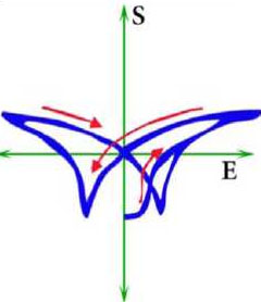
This indicates that a number of domains with dipoles oriented along the field have increased drastically. On further field increase the polarization again changes gradually. When the field is reversed the polarization decreases and at the negative coercive field (Ec - indicated by point 6) the polarization jumps to a negative value and continue decrease. The factors influencing these responses include stress, structural defects, and specifics of surfaces and interfaces [8]. The sample strain behavior during the same cycle of the electric field excitation is described in Figure 1b. The slopes of the lines, which are pointed with the arrows, represent the piezoelectric modulus d33. In actual samples the hysteretic curves deviate from the idealistic ones due to a number of reasons related to the sample polycrystalline nature, various structural imperfections, specifics of the experimental measurements.
EXPERIMENTAL SET-UP AND PFM MEASUREMENTS
The PFM setup realized in NEXT scanning probe microscope is shown in Figure 2. A conductive probe is brought into a contact with a sample and its load is adjusted by varying the deflection set-point.The piezoelectric activity is stimulated with an AC voltage applied between the tip and the sample that causes the periodical expansion or contraction of the sample.
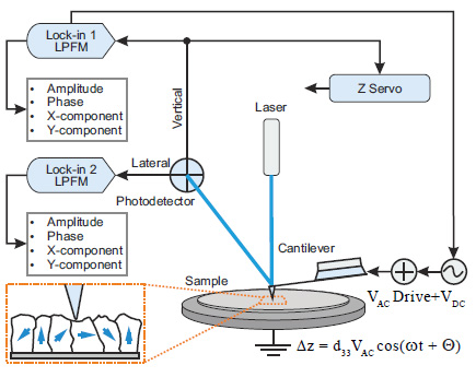
Figure 2. Sketch of Piezoresponse Force Microscopy set-up in scanning probe microscope NEXT
The changes of the sample dimensions are magnified by the cantilever deflection or bending and the latter are detected through the AC signals of different segments of the quadrant photodetector. The amplitude and phase of the vertical tip displacement are recorded by one of the lock-in amplifiers, and they are presented as VPFM amplitude and phase. Another amplifier is used for a detection of the amplitude and phase of the lateral response of the probe.
They are known as LPFM amplitude and phase. Instead of amplitude and phase one can measure amplitude cosine and sine components. Studies of local electromechanical properties can be performed at individual surface locations by recording the amplitude and phase signals when bias voltage is changing between the chosen limits of different polarities. By analogy with macroscopic studies of hysteretic loops of ferroelectrics, the amplitude versus bias voltage curve defines the local strain response and phase versus bias voltage dependence reflects the sample polarization behavior. The dependence of Acoswt versus bias voltage is known as the piezoresponse curve, which is often used in PFM studies. By analyzing local hysteresis loops, one learns about the piezoelectric properties of small piezo- and ferroelectric domains such as coercive voltages, nucleation voltages, forward and reverse saturation and permanent responses, as well as the effective work of switching, which is defined by the area embraced by the hysteresis loop [7]. The factors influencing these responses include stress, structural defects, and specifics of surfaces and interfaces [8]. Here it is worth mentioning several experimental details of practical PFM. They include a sample preparation, a choice of the probe and operational parameters such as a deflection set-point, amplitude and frequency of the electric excitation. Flat samples such as films are most suitable for PFM studies whereas the ceramic specimens need to be polished prior to imaging. A particular care should be taken for a removal of traces of abrasive from the sample surface and for preventing its external contamination. Typically, the conducting probes with stiffness in relatively large range: from 0.1 N/m to 40 N/m range can be applied for the piezo-resistive studies. The resonant frequencies of these probes are in the 10-400 kHz range and upon contact they are shifted to higher frequencies.
Another important parameter for measurements of small cantilever deflections and amplitudes is the optical sensitivity, which is the reversal of the probe length. Therefore, the shorter probes, which are stiffer than longer ones, do provide a better signal yet their applicability is directly related to mechanical strength of the sample. The samples examined in our studies were stiff enough that we can use the conducting probes with spring constant of ~40 N/m. This helps minimizing the undesirable cantilever-sample electrostatic effects, which can be substantial when soft probes are applied [7, 9]. In NEXT scanning probe microscope, PFM studies can be performed using the voltage in the (-50 V) – (+50 V) range depending on the sample nature and thickness. The use of lower voltages has an advantage of reducing the electrostatic force interactions, which might “contaminate” the piezo-response measurements. An electric excitation with low voltages (below 1 V) is particularly
important for spectroscopic measurements.
The electric AC field, which stimulates the sample piezo-response, in the tipsample- bottom electrode configuration can be generated by applying the bias either to the tip or the bottom electrode. An unwanted cross-talk between the driving signal and the piezo-response measurements can be avoided by supplying a bias voltage to the bottom electrode with a separate shielded wire. A choice of the frequency of the electric excitation is quite peculiar. One can either use the frequency well below
or at the probe contact resonance. In case of sub-resonant excitation the amplitude of the probe response directly follows the sample displacement. At the contact resonance the amplitude of the probe response (A) equals to d33 x Vac x Q, where Q is the quality factor of the contact resonance. The operation at the frequency of the contact resonance is more sensitive yet at these conditions the quantitative estimates of the piezoresponse are rather complicated due to signal amplification.
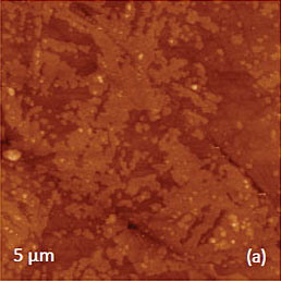
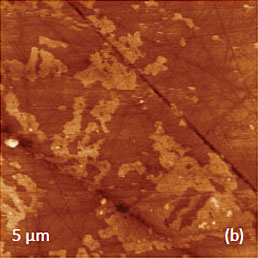
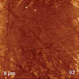
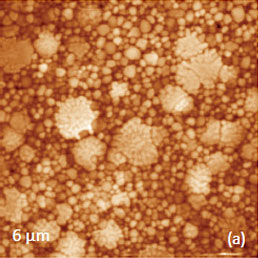
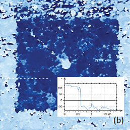
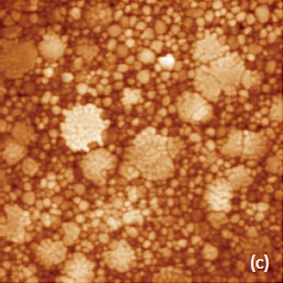
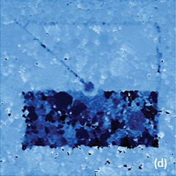
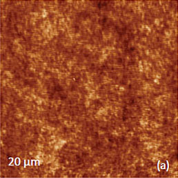
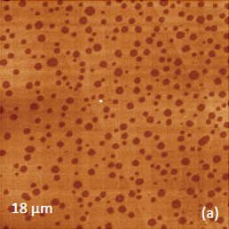
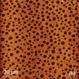
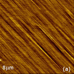
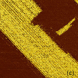
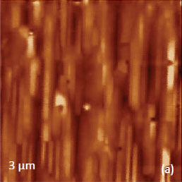
The mechanical tip-force control during scanning in the contact mode is performed by varying the deflection set-point. The chosen set-point should insure a stable tip-sample contact and prevents the sample damage. In some cases the scanning probe might swipe a surface contamination and this helps for establishing the direct contact with the examining sample. The above considerations are illustrated by imaging of a ceramic sample of PLZT in Figures 3a-d. The imaging of PLZT surface in the oscillatory amplitude modulation mode revealed a presence of surface adsorbate, which might originate from debris of polishing procedure or contamination during storage. This adsorbate layer, which is seen as bright patches in the height image, was gradually removed by a scanning probe during when PFM measurements in the contact mode were initiated, Figures 3a-3b.
The repetitive scanning of this area helps cleaning the sample surface, which exhibits a number of polishing lines, Figure 3c. Remarkably, the VPFM phase contrast, which reveals the domain morphology of the sample, is much cleaner on the areas free from the adsorbate, Figures 3c-d. Actually, in studies with the probe, which is 240 micron in length and has spring constant around 2 N/m, the piezo-response in the phase images was most noticeable with the operation at the contact resonance near 364 kHz. More peculiarities of the PFM measurements will be mentioned in the analysis of the data obtained on different samples.
SELECTED EXAMPLES
Lead Zirconate Titanate - PZT film
The PFM studies of the piezo-electrics and ferroelectrics include domain imaging, local spectroscopic studies and polarization procedures. PZT is one of the most known piezo-electric material with high d33 (100-500 pm/V), high remnant polarization and high dielectric constant.
This material is used for different actuators and PZT films serve as capacitors and data storage elements. Studies of PZT with scanning force microscopy were initiated almost 20 years ago [10]. We have performed PFM imaging of a PZT film, which is 4mm thick, using the conducting probes with spring constants of 2 N/m and 40 N/m. The
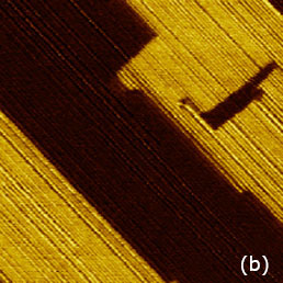
earlier study of this film showed that is has a columnar structure with random orientation of the grains with sub-micron lateral dimensions [8]. The height and PFM images of this sample obtained with the softer probe, Figures 4a-4c, reveal it grainy topography and the unique contrast of the VPFM phase image with the domains of opposite contrast. The cross-section taken along the several domains demonstrates that they differ by 180 degrees, Figure 4d. The contrast of the PFM amplitude image is quite dissimilar to the phase image and because it has a strong contribution of the sample topography. This effect is not unusual for the operation at the contact resonance in which topography variations are amplified as well as the sample piezo-response. A comparison of the topography image with the amplitude and phase maps for the PFM operation at the sub-resonant frequency with the stiff probe shows that the latter reflect the intrinsic domain structure of the sample that is not related to the surface topography, Figures 4e-f. The cross-section of a part of the phase image in Figure 4h reveals that the contrast reflects the reverse polarization of the domains. There are a large number of small domains with the diameter in the 50-100 nm range and some of them having opposite polarization.
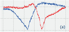
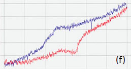
In the VPFM amplitude image some of the domains are surrounded by darker borders that can be assigned to the domain walls. Our observations of the domain morphology are consistent with those found in the studies of other PZT films [11]. The results of PFM spectroscopy measurements on the PZT films are illustrated by one set of the hysteresis curves in Figures 5a-c. The amplitude versus bias curve has a characteristic “butterfly” shape that is actually smoothened idealistic strain versus bias curve in Figure 1b. The polycrystalline nature of the sample is reflected in the experimental curves. The abrupt transitions in the phase curve take place at bias voltage around ±7 V. Depending on a location this coercive voltage varies and can reach ±15 V values.
This information is instructive when one wants to polarize the sample. One of the areas of PZT film was polarized by scanning the probe with DC bias voltage of 20 V, Figures 6a-b. The effect of polarization, its magnitude, and possible dissipation can be monitored in the PFM mode. The PFM imaging of a slightly larger area revealed that the polarized region exhibits a much stronger response compared to its non-polarized surrounding. This effect can be reversed by scanning the polarized area with the probe having negative bias voltage of -20 V. Such switching of the polarization was achieved in the top part of the polarized area as seen from Figures 6c-d.
Only the borders of the previously polarized area and the central position where the probe is rested between the images show the polarization traces. The height images do not exhibit any variations caused by the polarization procedure.
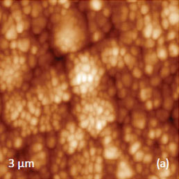
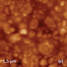
Lead lanthanum zirconate titanate - PLZT ceramics
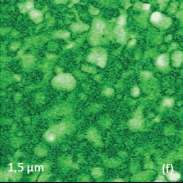
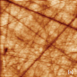
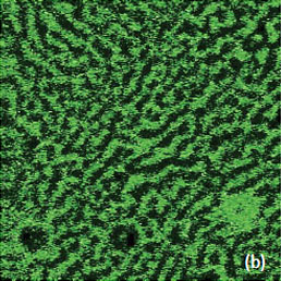
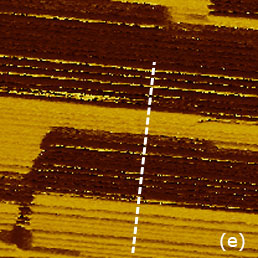
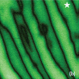
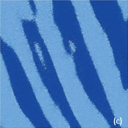
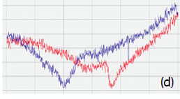
An application of PZT material for ferroelectric random access memories, which is justified by material large polarization and relatively reliable integration process, requires the improvement of the PZT fatigue and retention performance. The retention behavior is related to oxygen and Pb vacancies, and it can be improved by doping the material with lanthanum, niobium or other additives. A small addition (up to 10%) of donor dopant, like La3+ ions, enhance domain wall mobility leading to improved remnant polarization and also to lower dielectric constant and Curie point [12]. Characterization of PLZT material can be improved by PFM studies. As it was discussed above, a removal of a top contamination layer by a scanning probe opens a flat topography of the PLZT ceramic sample with a composition (Pb0.905La0.095 (Zr0.65Ti0.35)0.9575O3). The large-scale images (not shown here) show that the sample is composed of the grains of irregular hexagonal shape, which are typical for dense packing in hot-pressed ceramics. The largest grains have up to 10 microns in dimensions and a part of one of the grains is presented in Figures 7a-c. The height image of the sample reveals multiple polishing scratches (Figure 7a) whereas the domain morphology is clear distinguished in the VPFM amplitude and phase images (Figures 7b-c). Light and dark areas correspond to elongated wavy domains with opposite signs of the vertical polarization. This is evidenced by the 180-degrees steps seen in the phase profile in Figure 7d. The cross-section profile, which is made in the VPFM amplitude image, shows the depressed traces that represent the domain walls. These features are around 50 nm in width and they have a curved shape that is known as the domain roughness originated from the pinning of the domain walls by randomly distributed immobile defects. Domain walls should be flat in the absence of irregularities pinning the wall motion.
VPFM, Phase
Measurements of the domain walls dynamics and wall roughness of PLZT are described in more details in [13]. The PFM spectroscopy data, which were obtained for different amplitudes of the electric field excitation, are presented in Figures 8a-f. The shape of the amplitude, phase and piezo-response curves is similar to one obtained for PZT sample. The coercive voltages are below 10V. With the increase of the excitation voltage the signal-to-noise ratio of the curves improves yet it leads to a noticeable deviation of the phase of the piezo-response curve and increase of the effective work of switching.
An examination of the locations, which were used for harvesting spectroscopy data, showed the circular traces of local polarization, Figure 9a-b. Both effects need a further investigation combining the experimental results and finite element modeling of tip-sample electrostatic and electromechanical interactions.
Parallel Polarized Lithium Niobate, PPLN
Lithium niobate (LiNbO3) is the manmade ferroelectric material that is widely applied in acoustics transducers, delay lines, filters, optical amplitude and phase modulators, second harmonic generators and other technological products. The material is usually made as the macroscopic single crystal. At room temperature lithium niobate crystals exhibits a hexagonal symmetry with polarization along the c-axis, which arises from the displacement of cations (Li+ and Nb5+) with respect to oxygen planes along the c-axis. Thus, only two domain orientations are possible in lithium niobate (antiparallel 180º domains). For optical applications the crystals are often polished with the c-axis is perpendicular to the surface and polarized above the Curie point (1210°C) in different patterns using a lithographic mask, [14].
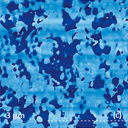
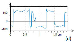
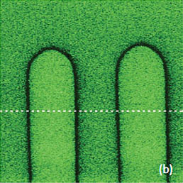
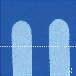
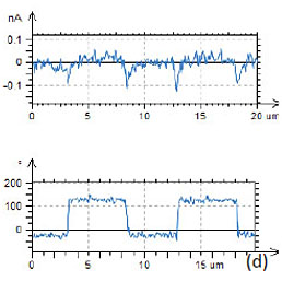
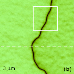
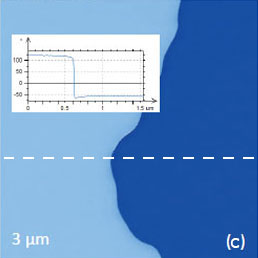
A similar specimen with parallel polarized domains is distributed by NT‑MDT SI as the standard for PFM training and applications. The height and PFM images of PPLN standard are shown in Figures 10a-c. A polished surface of this sample is very smooth and has no traces of the domain morphology, Figure 10a. The VPFM amplitude image reveals the domain pattern with two bright 5-μm wide “fingers”, Figure 10b. The image contrast reflects the minimal amplitude variations in the fingers and the matrix but well distinguished domain walls. The cross-section amplitude trace in Figure 10d indicates that the depressions representing the domain walls have a sub- 100 nm width. The pronounced phase contrast of ~180 degrees in Figure 10c points on the opposite polarization of the fingers and their surroundings.
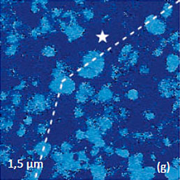
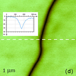
Due to possible imperfections of the lithographic mask, in some locations of the standard sample one can find domains with slightly rough walls as seen in Figures 11a‑d. This region with a smooth topography includes the differently polarized domains with high contrast amplitude and phase signals. The cross-section in the 1-μm amplitude image shows that the width of the wall at the half depth is ~50 nm. This value is larger than the domain wall thickness in the 5-15 nm range determined in single crystals of (Ba, Pb)TiO3 with electron microscopy [15]. The analysis of the broadening of the wall thickness includes the contributions of the probe dimensions and complex electrostatic interactions and depolarization field at the sample surface [16]. The questions regarding the spatial resolution of PFM measurements have been already addressed [17] but still is a subject of the debate.
Crystals of Triglycine Sulphate - TGS
Triglycine sulfate (TGS) is one of the most widely studied ferroelectric materials, which is broadly used together with its deuterated analog for infrared detectors. TGS is one of the few ferroelectrics known to exhibit a second-order phase transition and hence, to offer possibilities for the observation of this critical phenomenon very close to the transition temperature. Below the Curie temperature, TGS crystal exhibits antiparallel 180-degree domains, which are generally parallel to the b axis.
The domain shape of TGS is known to be of a lenticular shape, elongated in the direction parallel to the a axis. TGS is suitable for the study of static ferroelectric domain structures and domain dynamics by scanning probe microscope, because the direction of the spontaneous polarization is perpendicular to the cleaved surface (a–c plane). One of the first local studies of TGS was performed with the instrumental set-up similar to PFM but called as a dynamic contact operation of electrostatic force microscopy [17].
This work and the latter publication [18] presented a variety of TGS domain morphologies examined at different temperatures. These studies were performed with the probe scanned the sample in the contact mode with electric bias of 5 V at 40 kHz. The observation of the positively and negatively polarized domains, whose morphology does not affected by topographic features, was explained by detecting the electrostatic force variations caused by the surface charge density. This explanation is the alternative to the piezo-response effect. We have examined a single crystal of TGS of few millimeters in thickness. The crystal was cleaved to reveal a fresh surface (a-c plane). The height image of the surface reveals multiple patches with a depression slightly above 1 nm in depth, Figure 12a.
These features as well as small islands on the similar height can be assigned to the crystallographic steps in the b axis which has a crystallographic period of 1.27 nm. The VPFM phase image (Figure 12b) is featureless, most likely, because the crystal consists of equal number of positive and negative polarization domains with no piezoelectric effect.
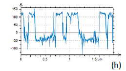
The situation changed after the crystal was heated to temperature above the material Curie point (49°C) and then cooled back to room temperature. As the height image of the annealed sample did not show changes (Figure 12c), the 180 degrees steps differentiate the domains of the opposite polarity appeared in the VPFM phase image, Figure 12d. The extended bright strips represent the parts of extended finger-like domains extended along the crystallographic a axis. The height and VPFM phase images of the larger area with 15-nm and 10-nm steps (Figures 12e-f) confirm that the domain morphology is practically independent from the surface topography. The slight traces of the topography cross-talk to the phase image are noticed only at the surface steps.
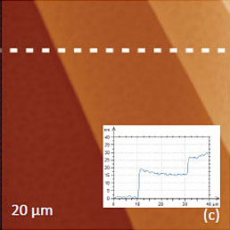
Bismuth Ferrite, BiFeO3 - BFO
Bismuth ferrite (BFO) is an inorganic compound with perovskite structure and one of the most promising magnetoelectric materials. BFO is multiferroic and it exhibits ferroelectricity, ferroelasticity and antiferromagnetism at room temperature. The control of magnetic ordering via applied electric fields has been demonstrated for single crystals and epitaxial thin films. Therefore, for future device application the mechanisms of magnetoelecric coupling at the nanoscale are studied intensively. Ferroelectric structure of BFO is rather complex. At the room-temperature the material is in the rhombohedral crystallographic phase and ferroelectric polarization
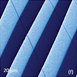
occurs along the pseudocubic [111] direction. This leads to eight equivalent polarization variants along the body diagonals of the pseudocubic unit cell and to domains separated by 71°, 109°, and 180° walls. The domain morphology and composition strongly depends on film growth parameters, and substrate and electrode configurations. Typically BFO films have [001] crystallographic orientation, therefore, the ferroelectric polarization should manifest itself in VPFM and LPFM
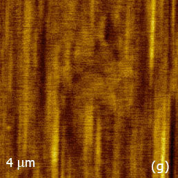
signals. Therefore, PFM can be applied for comprehensive characterization of anisotropic polarization and nanoscale switching mechanisms. The height and PFM images of the epitaxial BFO film, which were recorded at the different orientation of the sample striped morphology, are presented in Figures 13a-j. The probe was aligned along the Y-coordinate of the images. The domains with the opposite polarization are well distinguished in the VPFM and LPFM phase images, when they are recorded with the strips aligned in the ~45 degrees with respect to the probe, Figures 13a-c. When the strips were aligned perpendicular and parallel to the probe axis then the domain contrast was only enhanced respectively in VPFM phase image (Figures 13d-f) and in LPFM phase image (Figures 13g-j).
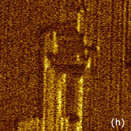
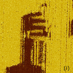
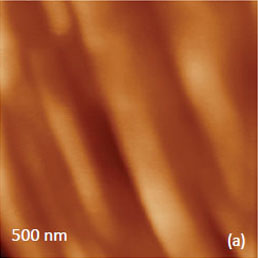
This effect can be explained by a strong in-plane piezoresponse of this sample, which is directed perpendicular to the strips. This response causes a buckling of the probe (strong normal force signal) when the probe is oriented perpendicular to the strips. When the probe is along the strips, the same effect causes a torque of the probe (strong lateral force signal). The cross-section profile of the trace in Figure 13f indicates that the observed domains differ by 180 degrees phase changes. In addition to the thin film we have examined a monodomain BFO material and the high-resolution images of this sample are presented in Figures 14a-c. The ferroelectric domains and their walls are well distinguished in the VPFM amplitude and phase images. The PFM spectroscopy data, which were obtained at one of the monodomain locations, Figures 14b,d‑f. The coercive voltages are around 5V.
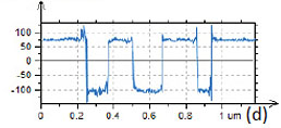
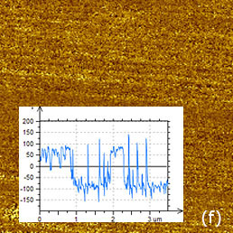
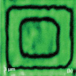
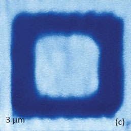
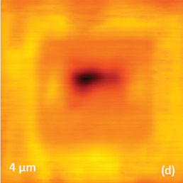
In studies of the sample polarization, a 2-micron region was polarized by the positively biased probe. This procedure was followed by its switching of the polarization at the smaller inside area. The height and PFM images of this location obtained after these exercises (Figures 15a-c) demonstrate that the polarization and its switching back were accomplished successfully without any modification of the sample topography. The polarization procedures, however, were accompanied by a deposition of positive and negative surface charges. This is evident from single-pass KPFM image, which was obtained at the polarized location, Figure 15d. The surface potential variations at this location were in the range of several hundreds of millivolts.
PFM CHALLENGES AND OPPORTUNITIES
The goal of the present Application Note is to demonstrate that the NEXT scanning probe microscope has the broad capabilities for collecting reliable highquality PFM imaging and spectroscopy data. This goal has been achieved in studies of five different materials. The presented results serve as the basis for more advanced research can be outlined in the following. Despite the wide application of PFM in the research of piezoelectric and ferroelectric materials, the imaging mechanism, particular the quantitative measurements and their interpretation meet a number of challenges. In the detailed analysis the additive contributions of the long-range electrostatic forces between the sample and the cantilever and the electromechanical tip-sample interactions to the total PFM response should be considered [3]. The sample-cantilever electrostatic forces lead to a constant background to the measured piezoresponse, and it can be minimized by using tall and high aspect-ratio tips. This suggestion needs to be verified with high-aspect probes having extra-long tips.
The use of the probe with T-shaped cantilever that carrying the tip whose position is offset from the cantilever axis enhances the torsional response of the probe to the in-plane piezoresponse. Therefore, such probe can be useful for studies the sample with strongly anisotropic polarization such as BFO films. The electroelastic contribution to the piezoresponse depends strongly on the contact interface between the tip and the surface, the shape, size, and material of the tip itself. Therefore, the use of metal-coated, stiff cantilever with large force (strong indentation) is most desirable for PFM imaging. This is also emphasized by the fact that these probes are short that provides high optical sensitivity for the detection of the small sample displacements. The only limitation of the stiff probes is their application to soft samples in the contact mode operation. Another concern for quantitative PFM measurement is the calibration of the instrument for quantitative studies of the piezoelectric coefficient. However, such measurements are complicated by the presence of a frequency dependent instrument background and other reasons. The needed efforts for accurate calibration and measurement of quantitative piezoelectric constants were proposed in [22].
In the future PFM applications it is worth expending the measurements to the broader frequency range to fully utilize the wide bandwidth (up to 8 MHz) of NEXT scanning probe microscope. In such work, higher resonances of the probes in the several MHz range can be applied for the detection of piezoresponse. The combination of PFM studies with other AFM-based electric modes such as singleand double-pass KPFM (Figure 15d) and dielectric response can be very informative in characterization
of ferroelectrics and might help to figure out the controversy described in [18].
ACKNOWLEDGEMENTS
Prof. A. Kholkin and Dr. I. Bdikin (both Aveiro University, Portugal), Dr. Jake Jokisaari (Prof. X. Pan Research Group, University of Michigan, Ann Arbor, USA) and Dr. R. Gainutdinov (Institute of Crystallography, Russian Academy of Sciences, Moscow, Russia) are acknowledged for kindly provided samples of PZT, PLZT, TGS and BFO, which were used in the studies described in this Application Note.
REFERENCES
1. F. Saurenbach, and B. D. Terris “Imaging of ferroelectric domain walls by force microscopy” Appl. Phys. Lett. 1990, 56, 1703–1705.
2. A. Gruverman, O. Auciello, and H. Tokumoto “Scanning Force Microscopy for the Study of Domain Structure in Ferroelectric Thin Films” J. Vac. Sci. Technol. B 1996, 14, 602-605.
3. S. V. Kalinin, and D. A. Bonnell “Imaging mechanism of piezoresponse force microscopy of ferroelectric surfaces” Phys. Rev. B 2002, 65, 125408.
4. A. L. Kholkin, S. V. Kalinin, A. Roelofs, and A. Gruverman, “Review of ferroelectric domain imaging by piezoresponse force microscopy” (in Scanning Probe Microscopy, S. Kalinin, A. Gruverman, Eds.), vol 1, pp. 173–214, Springer, New York, 2007.
5. D. Damjanovic “Ferroelectric, dielectric and piezoelectric properties of ferroelectric thin films and ceramics” Rep. Prog. Phys. 1998, 61, 1267–1324.
6. F. Jona, and G. Shirane “Ferroelectric crystals” 1993, Dover Publications Inc., New York.
7. S. Jesse, H. N. Lee and S. V. Kalinin “Quantitative mapping of switching behavior in piezoresponse force microscopy” Rev. Sci. Inst. 2006, 77, 073702-1-10.
8. I. K. Bdikin, A. L. Kholkin, A. N. Morozovska, S. V. Svechnikov, S.- H. Kim, and S. V. Kalinin “Domain dynamics in piezoresponse force spectroscopy: Quantitative deconvolution and hysteresis loop fine structure” Appl. Phys. Lett. 2008, 92, 182909-1-3.
9. S. Hong, J. Woo, H. Shin, J. U. Jeon, Y. E. Park, E. Colla, N. Setter, E. Kim and K. No “Principle of ferroelectric domain imaging using atomic force microscope” J. Appl. Phys. 2001, 89, 1377-1386.
10. K. Franke, J. Besold, W. Haessler, and C. Seegebarth “Modification and detection of domains on ferroelectric PZT films by scanning force microscopy” Surface Science Letters 1994, 302, L283-L288.
11. A. Gruverman, O. Auciello, and H. Tokumoto “Nanoscale investigation of fatigue effects in Pb(Zr,Ti)O3 films” Appl. Phys. Lett. 1996, 69, 3191-3193.
12. M. Plonska, and Z. Surowiak “Piezoelectric properties of X/65/35 PLZT ceramics dependent of the lanthanum (X) ions contents” Molec. Quant. Acoust. 2006, 27, 207-210.
13. N. A. Pertsev, D. A. Kiselev, I. K. Bdikin, M. Kosec, and A. L. Kholkin “Quasi-one-dimensional walls in ferroelectric ceramics: Evidence from domain dynamics and wall roughness measurements” J. Appl. Phys. 2011, 110, 052001-1-5.
14. W.-C. Yang, B. J., Rodriguez, A. Gruverman, and R. Nemanich “Polarization- dependent electron affinity of LiNbO3 surfaces” Appl. Phys. Lett. 2004, 85, 2316-2318.
15. M. D. Dennis and R.C. Bradt, “Thickness of 90° ferroelectric domain walls in (Ba,Pb)TiO3 single crystals” J. Appl. Phys. 74, 45, 1931- 1933.
16. S. V. Kalinin, S. Jesse, B. J. Rodriguez, E. A. Eliseev, V. Gopalan, and A. N. Morozovska “Quantitative determination of tip parameters in piezoresponse force microscopy” Appl. Phys. Lett. 2007, 90, 212905- 212907.
17. A. Roelofs, T. Schneller, K. Szot, and R. Waser “Piezoresponse force microscopy of lead titanate nanograins possibly reaching the limit of ferroelectricity” Appl. Phys. Lett. 2002, 81, 5231–5233. 18. J. W. Hong, K. H. Noh, S. Park, S. I. Kwun, and Z. G. Khim “Surface charge density and evolution of domain structure in triglycine sulfate determined by electrostatic-force microscopy” Phys. Rev. B 1998, 58, 5078-5084.
19. S. Shin, J. Baek, J. W. Hong, and Z. G. Khim “Deterministic domain formation observed in ferroelectrics by electrostatic force microscopy” J. Appl. Phys. 2004, 96, 4372-4377.
20. F. Zavaliche, P. Shafer, R. Ramesh, M. P. Cruz, R. R. Das, D. M. Kim, and C. B. Eom “Polarization switching in epitaxial BiFeO3 films” Appl. Phys. Lett. 2005, 87, 25902-25904.
21. H Béa, B. Ziegler, M Bibes, A Barthélémy, and P. Paruch “Nanoscale polarization switching mechanisms in multiferroic BiFeO3 thin films”
J. Phys.: Condens. Matter 2011, 23, 142201-142210.
22. T. Jungk, A. Hoffmann, and E. Soergel “Challenges for the determination of piezoelectric with piezoresponse force microscopy” Appl. Phys. Lett. 2007, 91, 253511–253513.