SCCM Studies of Microsctructure
+1-480-493-0093

SCCM Studies of Microsctructure

MDT-file: Download

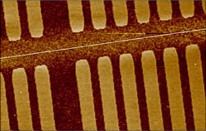
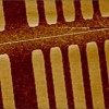
Test structure on the base of SiO2 stripes height 0.1µm grating on the silicon wafer. Ion implantation by boron with E=100 keV, annealing and SiO2 layer etching was employed.

On the resulting structure following images were obtained: Fig. 1 - Topography of test structure (contact mode AFM), Fig. 2. - Contact SCM image of the same area.


test_str_n300
test_str_n300
Topography of test structure (contact mode AFM)


size: 18x28x2 um
SPM principle: Constant Force mode
test_str_300a
Contact SCM image of the same area


size: 18x28 um
SPM principle: Scanning Capacitance Force Microscopy
Have more questions? Contact us
or fulfill a form and we will answer all your questions.