


Atomic Force Microscopy Studies of Mechanical and Electric Properties in the Contact Mode
Application Note 096 (pdf 3,3 Mb)
Sergei Magonov
NT-MDT Development Inc., Tempe, AZ 85284 USA
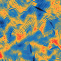
The height image of triblock copolymer. The 2 µm scan, contact mode
- Contact mode, introduced 30 years ago, is the pioneering AFM technique that is still a valuable partner for other methods
- Local mechanical studies in contact mode are demonstrated on polymer blends
- Mapping of electrostatic force response in contact mode helps to characterize the electrically-active materials
INTRODUCTION
Atomic force microscopy (AFM) was developed in 1986 [1], and the first innovations of this technique were associated with contact mode operation. In this mode the tip-sample force is detected by the bending of a cantilever that carries a sharp tip interacting with the sample surface. The cantilever deflection is directly related to the tip-sample force, and surface profiling is performed with the tip staying in permanent contact with the sample while the cantilever deflection is kept constant. A choice of the set-point deflection plays an important role as it should be lowered for studies of soft and fragile surfaces or increased if one is interested in finding surface locations of different stiffness.
With the broadening of AFM applications, the limitations of contact mode in applications with soft materials were identified, and as a result, oscillatory modes help overcome this hurdle. Nevertheless contact mode is a valuable technique for the examination of large number of samples. Below we will illustrate this by examples of local mechanical and electric properties studies in this mode. The latest capabilities are enhanced with the use of oscillatory means and lock-in amplifiers for measurements of dynamic probe responses to different perturbations. Our experimental results show that contact mode remains an appreciated counterpart in family of AFM techniques.
DEALING WITH MECHANICAL STUDIES
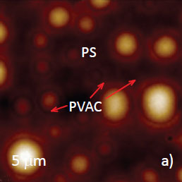
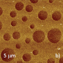
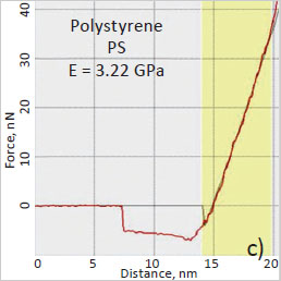
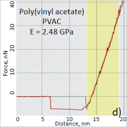
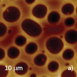
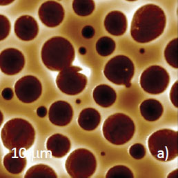
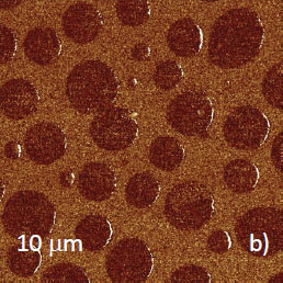
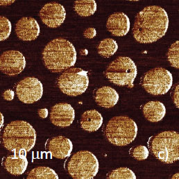
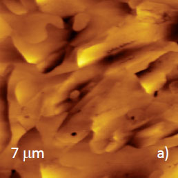
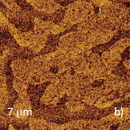
The use of contact mode is directly related with stiffness of the probe and mechanical properties of a sample. For example, AFM probes with spring constant in the 2-5 N/m range can be applied to relatively stiff polymers with elastic modulus above 1 GPa. The related example is shown in Figure 1 with height, deflection and lateral force images of immiscible blend of atactic polystyrene (PS) and poly(vinyl acetate) (PVAC). The height image reproduces surface topography, whereas the lateral force image is related to local adhesion, and it contrast differentiates the circular inclusions of PVAC from a matrix enriched in PS. The applied probe was stiff enough to deform the blend components as reflected by the deflection-versus-distance curves [2-3].
The fit of the curves with elastic deformation model (DMT) showed elastic modulus of E=3.22 GPa for the matrix and E=2.48 GPa for the circular domains. The data correlates well to macroscopic elastic moduli of PS and PVAC, resp.
The use of the force curves for extraction of elastic modulus can be extended to multiple sites to provide the elastic modulus maps. However, the process is slow and dynamic modes (force modulation [4] and contact resonance [5]) were employed for mechanical studies in contact mode.
Height
Lateral Force
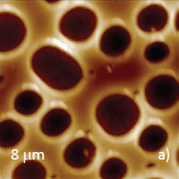
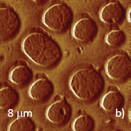
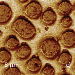
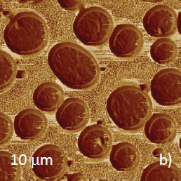
In force modulation, which was introduced in 1992 [4], the probe in continuous contact with a sample is additionally driven into a periodical oscillation at frequency (ω) below its resonance. In this case the probe and the cantilever are moving vertically, and as the tip indents a hard location it bends stronger than on a softer spot. This situation is shown in a sketch (Figure 2) and in an example in Figure 3. As seen from height image (Figure 3a), a layer of polymer blend of syndiotactic polystyrene (sPS) and poly(vinyledene difluoride) - PVDF on Si is characterized by a matrix with depressed inclusions. A dissimilar contrast of the locations is observed in the lateral force image (Figure 3b) as well as in the map of amplitude at 3 kHz (Figure 3c). Large amplitudes (bright contrast) were obtained at matrix locations. This allows the assignment of the matrix to sPS, whose elastic modulus (E=7 GPa) is higher than that of PVDF (E=2 GPa).
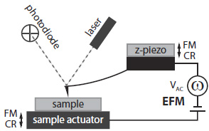
Figure 2. Sketch of the modulation techniques for studies of mechanical and electric properties in the contact mode. FM – force modulation, CR – contact resonance, EFM – electric force microscopy
Height
Lateral Force
Amplitude, 3 kHz
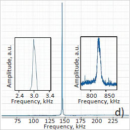
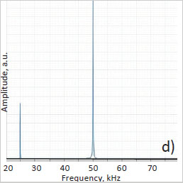
In a separate experiment this sample was examined in the contact resonance mode, Figure 4a‑b. For the applied Si probe with k=4.3 N/m and free resonance at 140 kHz the contact resonance was found at 835 kHz, Figure 3d.
The blend components are revealed in the height image and amplitude map. In this mode, the frequency shifts of contact resonance can also be used for discerning the locations of different stiffness.
Height
Amplitude, 835 kHz
PROBING ELECTROSTATIC FORCE EFFECTS
Since first AFM applications it was suggested for probing local electric properties [6]. When the conducting probe stays in contact with electrically active sample, electrostatic force between these electrodes can be induced by AC bias applied at frequency below the probe resonance, Figure 5d.
Height
Amplitude, 25 kHz
Amplitude, 50 kHz
The capacitance-like contact leads to the probe oscillation not only at the excitation frequency but also at its second harmonic. The amplitudes of both frequencies can be applied for visualization of locations with different electric response. This is demonstrated by observing the electric-dipole rich locations of PVDF in the sPS matrix (Figures 5a-c) and domains of different metals of incomplete Bi/Sn alloy (Figures 6a-b). These examples show that electric force microscopy in contact mode complements the single-pass and double-pass electric studies in amplitude modulation mode.
Height
Amplitude, 25 kHz
Height
Amplitude, 50 kHz
Phase, 50 kHz
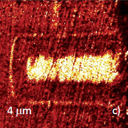
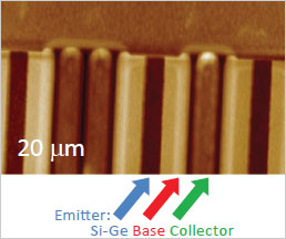
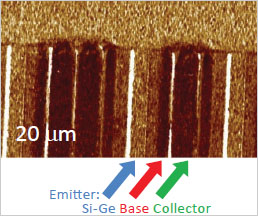
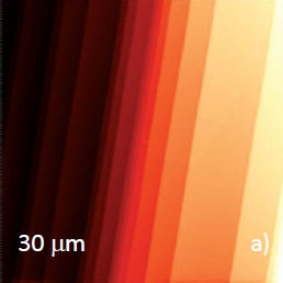
Similar EFM measurements can be conducted on rigid samples with semiconductor structures. In the first example, the images were collected on a polished surface of the CMOS (complimentary metal-oxide semiconductor) structure. The height image (Figure 7a) shows a relatively smooth topography with multiple traces of polishing grooves. The doped structure, which is not seen in the height image, has been revealed with highest contrast in amplitude and phase maps of 2nd harmonic of the excitation frequency (Figures 7b-c). The second example is taken from studies of heterojunction bipolar transistor, in which the base, collector and emitter are made of differently doped materials (Si n+, Si p+, and Si-Ge, resp.).
Topographic profiles of these elements are visualized in the height image (Figure 8a). The amplitude image (Figure 8b), which is recorded at the excitation frequency of 25 kHz, exhibits different contrasts of the base, collector and emitter. This observation is useful in the search for the AFM-based technique that will provide the most reliable identification of the dopant type and level in the semiconductor structures.
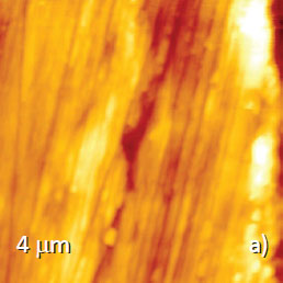
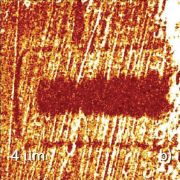
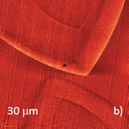
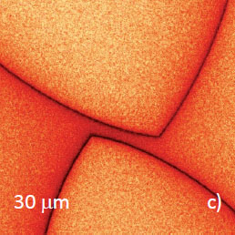
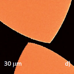
Further extension of local measurements of material properties this contact mode has developed into piezoresponse force microscopy (PFM) [7] that is broadly applied for studies of piezoelectric and ferroelectric materials. Such studies are illustrated by images obtained on crystalline surface of triglycine sulphate (TGS) – one of best explored materials [8].
The examined sample was cleaved to open new crystalline surface and then subjected to heating above Curie point (49°C) and slow cooled to room temperature. The surface possesses multiple layers with a height of 1.26 nm equal to the crystallographic b-constant, Figure 9a. The lateral force image (Figure 9b) and, particularly, the amplitude and phase maps (Figures 9c-d), which were recorded at the excitation frequency, are quite different from the surface topography. They expose parts of two uniaxial ferroelectric domains with a lens-like shape.
Height
Amplitude, 25 kHz
The transistor elements are indicated with the color arrows
Height
Lateral Force
Amplitude, 25 kHz
Phase, 25 kHz
CONCLUSIONS
Several applications of the contact mode, which are collected in this document, became possible by combining this 30-year old mode with the recording of stimulated oscillatory behavior of the probe at multiple frequencies using lock-in amplifiers. This combination keeps the contact mode as the valuable counterpart of other AFM modes for comprehensive characterization of materials.
REFERENCES
[1] G. Binnig, C. Quate, and Ch. Gerber, Phys. Rev. Lett. 56, 930 (1986).
[2] A. L. Weisenhorn, P. K. Hansma, T. R. Albrecht, and C. F. Quate, Appl. Phys. Lett. 54, 2651 (1989).
[3] N. A. Burnham and R. J. Colton, J. Vac. Sci. Technol.A7, 2906 (1989).
[4] P. Maivald, H.-J. Butt, S. A. C. Gould, C. B. Prater, D. Drake, G. Gurley, V. B. Elings, and P. K. Hansma Nanotechnology 2, 13 (1991).
[5] U. Rabe and W. Arnold, Appl. Phys. Lett. 64, 1493 (1994).
[6] Y. Martin, D. A. Abraham, and H. K. Wickramasinghe, Appl. Phys. Lett., 52, 1103 (1988).
[7] A. L. Kholkin, S. V. Kalinin, A. Roelofs, and A. Gruverman, in Scanning Probe Microscopy (S. Kalinin, A. Gruverman, Eds.) 1, 173 Springer, New York (2007).
[8] H. Haefke, R. Luethi, K.-P. Meyer, and H.-J. Guentherodt, Ferroelectrics 151, 143 (1994).