Scientific Digest Scanning Near-field Optical Microscopy
11.11.2020
Scientific Digest SNOM (pdf 1.5 Mb)
Scanning near-field optical microscopy (SNOM) enables studying a sample’s optical properties with resolution far beyond the diffraction limit. Sample fluorescence, light emission, transmission, scattering etc. can be mapped with the spatial resolution down to tens of nanometers.
Two main approaches to the near-field microscopy exist: aperture type SNOM and apertureless techniques.
In the first case, a subwavelength size aperture on a scanning tip is used as an optical probe. This is usually an opening in a metal coating of either an optical fiber tip or of a cantilever. Spatial resolution in the aperture type SNOM is, in general, determined by the aperture diameter.
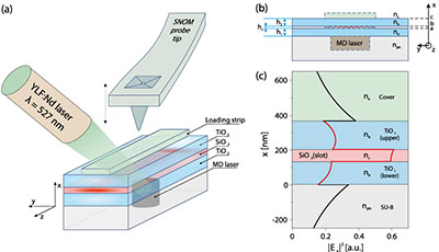
Strip-Loaded Horizontal Slot Waveguide for Routing Microdisk Laser Emission

Marina Fetisova, Natalia Kryzhanovskaya, Igor Reduto, Valentina Zhurikhina, Olga Morozova, Aleksandr Raskhodchikov, Matthieu Roussey, Ségolène Pélisset et al.
Journal of the Optical Society of America B 37, 1878-1885 (2020)
https://doi.org/10.1364/JOSAB.391993
Journal of the Optical Society of America B 37, 1878-1885 (2020)
https://doi.org/10.1364/JOSAB.391993
A strip-loaded horizontal slot waveguide is used for routing the emission of a microdisk laser. The active region of the laser contains InAs/InGaAs/GaAs quantum dots operating inCWmode under optical pumping. Although the quantum dots emit in a broad range, the laser emission is single mode with λ=1290 nm. Atomic layer deposition is used for the fabrication of the TiO2=SiO2=TiO2 slot waveguide covering the 10 μm-diameter disk. The horizontal slot waveguide covers the microdisk and traps the emission in the fundamental TM mode of the three-stack layer. Once light is localized inside this planar waveguide, a loading strip creates an effective index difference, which is sufficient to confine the mode laterally and leads to the guiding of the lasing emission. An analytical model for the five-layer horizontal planar slot waveguide was developed in order to optimize the slot waveguide according to the operation wavelength of the microlaser and the different materials involved. Scanning near-field optical microscopy is used to observe the propagation of light within the waveguide and confirm the mode coupling into it and therefore the guiding along the loading strip.
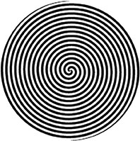
Two-Petal Laser Beam near a Binary Spiral Axicon with Topological Charge 2

Kotlyar, V. V., Stafeev, S. S., Nalimov, A. G., Schulz, S., & O’Faolain, L.
Optics and Laser Technology, 2019, 119, 105649
https://doi.org/10.1016/j.optlastec.2019.105649
Optics and Laser Technology, 2019, 119, 105649
https://doi.org/10.1016/j.optlastec.2019.105649
We were the first to notice that although in the immediate vicinity of a spiral axicon with m>0 there is no light ring, there is an intensity pattern composed of several intensity petals, whose number is equal to the axicon topological charge, m. We experimentally demonstrate that a spiral axicon with the topological charge m=2 and numerical aperture NA≈0.6, operating at a 532-nm wavelength and fabricated by electron lithography, generates a two-petal (TP) laser beam rotating in the near-field (several micrometers away from the microaxicon surface). The rotation rate attained is higher than any that has been reported to date. It is worth noting that the higher the rotation rate of the TP-beam, the higher the axial resolution of an optical system that can be achieved without increasing its NA. Because a small on-axis shift of a point object leads to a large angle of rotation of its TP-image.
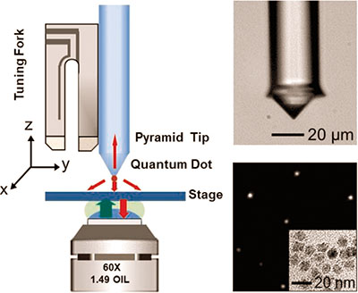
Quantum dot Decorated Nano-Pyramid Fiber Tip for Scanning Near-Field Optical Microscopy

Pan, B., Yang, Y., Bian, J., Hu, X., & Zhang, W.
Optics Communications, 2019, 445, 273–276
https://doi.org/10.1016/j.optcom.2019.04.053
Optics Communications, 2019, 445, 273–276
https://doi.org/10.1016/j.optcom.2019.04.053
We report a new type of nano-optical tip, the quantum dot decorated nano-pyramid fiber tip, for scanning near-field optical microscopy. The nano-pyramid tip has a large apex angle (70.5 degree), and consequently exhibits a significant improvement (17-fold) of the signal collection efficiency compared to conventional tapered fiber tips. Moreover, thanks to the template-based fabrication method and the surface treatment technique, the quantum-dot decorated nano-pyramid tip enjoys a clean and smooth surface, and can be produced with high accuracy and high reproducibility. Experimental results show that, with the nano-pyramid tip, the optical field distribution of a photonic nanostructure can be mapped with a 20 nm resolution (λ/20). It provides a powerful and reliable tool for near-field optical measurements.
Lasing at Topological Edge States in a Photonic Crystal L3 Nanocavity

Han, C., Lee, M., Callard, S., Seassal, C., & Jeon, H.
Light: Science & Applications, 2019, 8, 40
https://doi.org/10.1038/s41377-019-0149-7
Light: Science & Applications, 2019, 8, 40
https://doi.org/10.1038/s41377-019-0149-7
Topological photonics have provided new insights for the manipulation of light. Analogous to electrons in topological insulators, photons travelling through the surface of a topological photonic structure or the interface of two photonic structures with different topological phases are free from backscattering caused by structural imperfections or disorder. This exotic nature of the topological edge state (TES) is truly beneficial for nanophotonic devices that suffer from structural irregularities generated during device fabrication. Although various topological states and device concepts have been demonstrated in photonic systems, lasers based on a topological photonic crystal (PhC) cavity array with a wavelength-scale modal volume have not been explored. We investigated TESs in a PhC nanocavity array in the Su–Schrieffer–Heeger model. Upon optical excitation, the topological PhC cavity array realised using an InP-based multiple-quantum-well epilayer spontaneously exhibits lasing peaks at the topological edge and bulk states. TES characteristics, including the modal robustness caused by immunity to scattering, are confirmed from the emission spectra and near-field imaging and by theoretical simulations and calculations.
Near-Field Imaging of Surface-Plasmon Vortex-Modes around a Single Elliptical Nanohole in a Gold Film

Triolo, C., Savasta, S., Settineri, A., Trusso, S., Saija, R., Agarwal, N. R., & Patanè, S.
Scientific Reports, 2019, 9, 5320
https://doi.org/10.1038/s41598-019-41781-2
Scientific Reports, 2019, 9, 5320
https://doi.org/10.1038/s41598-019-41781-2
We present scanning near-field images of surface plasmon modes around a single elliptical nanohole in 88 nm thick Au film. We find that rotating surface plasmon vortex modes carrying extrinsic orbital angular momentum can be induced under linearly polarized illumination. The vortex modes are obtained only when the incident polarization direction differs from one of the ellipse axes. Such a direct observation of the vortex modes is possible thanks to the ability of the SNOM technique to obtain information on both the amplitude and the phase of the near-field. The presence of the vortex mode is determined by the rotational symmetry breaking of the system. Finite element method calculations show that such a vorticity originates from the presence of nodal points where the phase of the field is undefined, leading to a circulation of the energy flow. The configuration producing vortex modes corresponds to a nonzero total topological charge (+1).

3D ITO-Nanowire Networks as Transparent Electrode for All-Terrain Substrate
Li, Q., Tian, Z., Zhang, Y., Wang, Z., Li, Y., Ding, W., Wang, T., & Yun, F.
Scientific Reports, 2019, 9, 4983
https://doi.org/10.1038/s41598-019-41579-2
Scientific Reports, 2019, 9, 4983
https://doi.org/10.1038/s41598-019-41579-2
A 3D ITO nanowire network with high quality by using polystyrene as an assisted material has been prepared, demonstrating superior optoelectronic performances with a sheet resistance of 193 Ω/sq at 96% transmission. Both remarkable flexibility tested under bending stress and excellent adhesion applied on special terrain substrate have been achieved. This method has led to a full coverage of micro-holes at a depth of 18 µm and a bottom spacing of only 1 µm, as well as a perfect gap-free coverage for micro-tubes and pyramid array. It has been proved that this 3D ITO nanowire network can be used as a transparent conductive layer for optoelectronic devices with any topography surface. Through the application on the micro-holes, -tubes and -pyramid array, some new characteristics of the 3D ITO nanowires in solar cells, sensors, micro-lasers and flexible LEDs have been found. Such 3D ITO nanowire networks could be fabricated directly on micro-irregular substrates, which will greatly promote the application of the heterotypic devices.
Scanning Near-Field Optical Nanospectrophotometry: a New Method for Nanoscale Measurements of the Absorption Spectra of Single Nanoobjects

Mochalov, K. E., Solovyeva, D. O., Vaskan, I. S., & Nabiev, I. R.
Technical Physics Letters, 2019, 45(2), 138–141
https://doi.org/10.1134/S1063785019020287
Technical Physics Letters, 2019, 45(2), 138–141
https://doi.org/10.1134/S1063785019020287
A new experimental method for nanoscale measurements of the absorption spectra of single nanoobjects has been developed based on scanning near-field optical microspectroscopy (SNOM) and nanospectrophotometry (NSP). The main distinctive feature of the proposed SNOM-NSP technique consists in depositing a sample onto a coverglass followed by its probing in the total internal reflection spectroscopy mode. This approach allows the number of analyzed samples to be significantly increased and provides the possibility of combining measurements with other optical techniques. The proposed SNOM-NSP method has been successfully used for studying single plasmonic nanoparticles and their complexes with Rhodamine 6G dye.
Subwavelength Grating-Based Spiral Metalens for Tight Focusing of Laser Light

Kotlyar, V. V., Stafeev, S. S., Nalimov, A. G., & O’faolain, L.
Applied Physics Letters, 2019, 114(14)
https://doi.org/10.1063/1.5092760
Applied Physics Letters, 2019, 114(14)
https://doi.org/10.1063/1.5092760
In this paper, we investigate a 16-sector spiral metalens fabricated on a thin film (130 nm) of amorphous silicon, consisting of a set of subwavelength binary diffractive gratings and with a numerical aperture that is close to unity. The metalens converts linearly polarized incident light into an azimuthally polarized optical vortex and focuses it at a distance approximately equal to the wavelength of the incident light, λ=633 nm. Using a scanning near-field optical microscope, it is shown experimentally that the metalens forms an elliptical focal spot with diameters smaller than the diffraction limit: FWHMx=0.32λ (±0.03λ) and FWHMy=0.51λ (±0.03λ). The experimental results are close to those of a numerical simulation using the FDTD method, with FWHMx=0.37λ and FWHMy=0.49λ. The technological errors due to manufacturing were taken into account in the simulation. This is the smallest focal spot yet obtained with a metalens.
Luminescence Landscapes of Nitrogen-Vacancy Centers in Diamond: Quasi-Localized Vibrational Resonances and Selective Coupling

Su, Z., Ren, Z., Bao, Y., Lao, X., Zhang, J., Zhang, J., Zhu, D., Lu, Y., Hao, Y., & Xu, S.
Journal of Materials Chemistry C, 2019, 7(26), 8086–8091
https://doi.org/10.1039/c9tc01954e
Journal of Materials Chemistry C, 2019, 7(26), 8086–8091
https://doi.org/10.1039/c9tc01954e
Among the known color centers of diamond, the
nitrogen-vacancy (NV) center composed of a substitutional nitrogen and its nearest carbon vacancy could be the most promising photon emitter. In this work, we present the
micro-photoluminescence (μ-PL) landscapes of two quasi-localized vibrational resonances (~45 and ~63 meV) associated with the neutral (NV0) and negative (NV−) NV centers, respectively. A symmetric electron–phonon coupling theoretical model was used to simulate the μ-PL spectra with vibronic structures, so that the effective phonon densities of states and Huang–Rhys factors could be obtained for the two charge states of the NV centers. Our study also reveals that the perfect lattice optical phonon mode plays a more significant role in the luminescence of the NV0 state, whereas the quasi-localized vibrational resonance plays the dominant role in the case of NV-.
Manipulation for Superposition of Orbital Angular Momentum States in Surface Plasmon Polaritons

Zhang, Y. Q., Zeng, X. Y., Ma, L., Zhang, R. R., Zhan, Z. J., Chen, C., Ren, X. R., He, C. W., Liu, C. X., & Cheng, C. F.
Advanced Optical Materials, 2019, 7(18), 1–9
https://doi.org/10.1002/adom.201900372
Advanced Optical Materials, 2019, 7(18), 1–9
https://doi.org/10.1002/adom.201900372
Superposition of orbital angular momentum (OAM) states and the structured intensity are providing new approaches for manipulating optical information and light–matter interactions. While superposition of OAMs in free space has been well studied, further extensions to surface plasmon polariton (SPP) confined in near-field would be crucial for miniaturing and integrating platforms. Here, the plasmonic metasurfaces consisting of rotated nanoslits arranged in a segmented spiral are proposed to realize the superposition of two SPP OAM states. The nanoslit rotation and the azimuthally variant radius of segmented spiral introduce the spin-dependent geometric phase and position-dependent dynamic phase, respectively, and combination of two phases generates two incorporating OAM states. By designing metasurfaces with different parameters, the superposition of two different OAM states and complex structured pattern can be achieved. The four degrees of freedom including rotation order q, spiral order m, initial orientation angle α0, and incident circular polarization σ, enable the superposition of SPP OAM states in a straightforward and flexible manner.
Probing the Photonic Spin–Orbit Interactions in the Near Field of Nanostructures

Lin Sun, Benfeng Bai, Jia Wang, Mingqian Zhang, Xiaomeng Zhang, Xu Song, Lingling Huang
Advanced Functional Materials, 2019, 29(32), 1902286
https://doi.org/10.1002/adfm.201902286
Advanced Functional Materials, 2019, 29(32), 1902286
https://doi.org/10.1002/adfm.201902286
Photonic spin–orbit interactions (SOI) provide a new design paradigm of functional nanomaterials and nanostructures, and have especially accelerated advances in spin–orbit photonics. The berry phase or the geometric phase, a salient property of SOI, plays a vital role in this process. Thus, the characterization of photonic SOI processes together with the Berry phase is highly demanded for studies such as the optical spin-Hall effect, spin-to-vortex conversion, and Rashba effect. Here, a spin-selective and phase-resolved near-field microscopic method is proposed and experimentally demonstrated for real-time probing and direct visualization of photonic SOI at mesoscale, and a 3D tomographic technique for imaging the spatial evolutions of the optical phases is also properly realized. By analyzing a metallic metasurface as a spin-to-vortex conversion platform, the abrupt geometric phase and the spatially evolutional dynamic phases are directly measured.
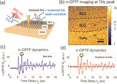
Photo-Induced Terahertz Near-Field Dynamics of Graphene/InAs Heterostructures

Ziheng Yao, Vyacheslav Semenenko, Jiawei Zhang, Scott Mills, Xiaoguang Zhao, Xinzhong Chen, Hai Hu, Ryan Mescall, Thomas Ciavatti, Stephen March, Seth R. Bank, Tiger H. Tao, Xin Zhang, Vasili Perebeinos, Qing Dai, Xu Du, and Mengkun Liu
Optics Express, 2019, 27(10), 13611-13623
https://doi.org/10.1364/OE.27.013611
Optics Express, 2019, 27(10), 13611-13623
https://doi.org/10.1364/OE.27.013611
In this letter, we report optical pump terahertz (THz) near-field probe (n-OPTP) and optical pump THz near-field emission (n-OPTE) experiments of graphene/InAs heterostructures. Near-field imaging contrasts between graphene and InAs using these newly developed techniques as well as spectrally integrated THz nano-imaging (THz s-SNOM) are systematically studied. We demonstrate that in the near-field regime (λ/6000), a single layer of graphene is transparent to near-IR (800 nm) optical excitation and completely “screens” the photo-induced far-infrared (THz) dynamics in its substrate (InAs). Our work reveals unique frequency-selective ultrafast dynamics probed at the near field. It also provides strong evidence that n-OPTE nanoscopy yields contrast that distinguishes single-layer graphene from its substrate.
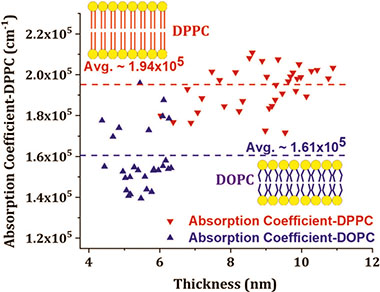
Visualization and Measurement of the Local Absorption Coefficients of Single Bilayer Phospholipid Membranes Using Scanning Near-Field Optical Microscopy

Siddiquee, A. M., Hasan, I. Y., Wei, S., Langley, D., Balaur, E., Liu, C., Lin, J., Abbey, B., Mechler, A., & Kou, S.
Biomedical Optics Express, 2019, 10,(12), 6569
https://doi.org/10.1364/boe.10.006569
Biomedical Optics Express, 2019, 10,(12), 6569
https://doi.org/10.1364/boe.10.006569
Here we report the results of shear-mode thicknesses and absorption coefficient measurements made on neat membranes using scanning near-field optical microscopy (SNOM). Biomimic neat membranes composed of two different types of phoshpholipid molecules: 1,2-dioleoyl-sn-glycero-3-phosphocholine (DOPC) and 1,2-dipalmitoyl-sn-glycero-3-phosphocholine (DPPC) were found to exhibit different absorption coefficients under the SNOM. The localization of the lipids could be identified and correlated to the morphology of the membrane domains indicating that SNOM can be an effective and accurate approach for the label-free characterization of the structure-function relationships in cell membranes.
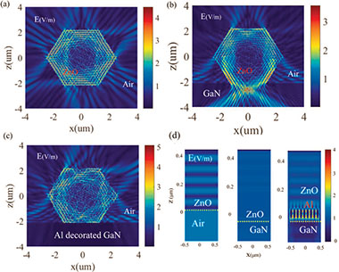
Interfacial Control of ZnO Microrod for Whispering Gallery Mode Lasing

Fiefei Qin, Chunxiang Xu, Dang Yuan Lei, Siqi Li, Jin Liu, Qiuxiang Zhu, Qiannan Cui, Daotong You, A. Gowri Manohari, Zhu Zhu, and Feng Chen
ACS Photonics 2018, 5, 6, 2313–2319
https://doi.org/10.1021/acsphotonics.8b00128
ACS Photonics 2018, 5, 6, 2313–2319
https://doi.org/10.1021/acsphotonics.8b00128
Energy loss control at interfacial areas is a significant issue to improve the optical performance of hybrid optical resonant cavities. In this work, we analyzed the simulated electric field intensity to predict the optical loss or gain in ZnO microrod cavity interfaced with both pristine and Al nanoparticles decorated GaN gratings. A single ZnO microrod was placed on GaN gratings to compose three interfacial configurations, these are, ZnO/Air, ZnO/GaN, and ZnO/Al/GaN, their lasing behaviors were investigated experimentally. Experimental results indicate that the lasing intensity, threshold power, and quality factor all depend on interfacial gain and loss. Through introducing the localized surface plasmon resonance (LSPR) of Al nanoparticles at interface areas, improved lasing performance was observed for the ZnO/Al/GaN hybrid structure. Furthermore, the LSPR coupling mechanism responsible for the observed lasing improvement was revealed by the scanning near-field optical microscopy (SNOM) and time-resolved photoluminescence (TRPL) spectroscopy.
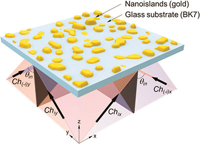
Metallic 3D Random Nanocomposite Islands For Near-Field Spatial Light Switching

Son, T., Moon, G., Lee, H. & Kim, D.
Advanced Optical Materials, 2018, 6(10), 1701219
https://doi.org/10.1002/adom.201701219
Advanced Optical Materials, 2018, 6(10), 1701219
https://doi.org/10.1002/adom.201701219
Random nanocomposite islands have drawn significant interest for diverse applications due to extreme simplicity of fabricating nanoscale structures. In this paper, the near-field characteristics of random nanoislands produced by spatial light switching are investigated, with light incidence switching among 14 incident channel modes. The results show that localized light fields are displaced from nanoislands almost linearly with the incident angle of channels. Also, light fields rotate in a manner aligned to the direction of light incidence. Ten-channel spatial switching is found to provide coverage of near-fields on the surface close to 90%. The numerical data are experimentally validated using fluorescent imaging and near-field scanning optical microscopy. The results suggest the possibility of using random nanoislands for high performance imaging such as superresolution microscopy and molecular detection techniques.
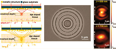
Three-Dimensional Resolvable Plasmonic Concentric Compound Lens: Approaching the Axial Resolution from Microscale to Nanoscale
Chang, K., Chen, Y., Chang, W. & Lee, P.
ACS Photonics 2018, 5, 3, 834–843
https://doi.org/10.1021/acsphotonics.7b01003
ACS Photonics 2018, 5, 3, 834–843
https://doi.org/10.1021/acsphotonics.7b01003
We propose the design and working principle of a plasmonic concentric compound lens (CCL) comprising inner circular nanoslits and outer circular nanogrooves. Dual-wavelength operations have been achieved for 650 and 750 nm at nanoscale and microscale focal lengths along with their depth of focus (DOF). By tuning the arrangement of nanogrooves, the axial resolution can be modulated and the narrowest DOF is achieved by a design of gradually decreasing groove width. For the ultrahigh tunability of axial resolution, DOF over 400 nm for both working wavelengths is also achieved. We not only developed an approximate-perturbed-focus model for explaining the performance of DOF but also found an extraordinary way to improve the resolution. The enhanced resonance of central disk as nannoantenna in CCL also has great influence on nanofocusing with different deigns of outer nanogrooves. This work provides new sight of focusing ability governed by the general optical nanogrooves. The optimized CCL shows excellent focusing performance with a lateral resolution down to 0.32λ (λ=650 nm), which is the best resolving ability achieved thus far in the near field region with a long focal length up to 500 nm.
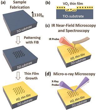
Controlling Phase Separation in Vanadium Dioxide thin Films Via Substrate Engineering

The strong electron-lattice interactions in correlated electron systems provide unique opportunities for altering the material properties with relative ease and flexibility. In this Rapid Communication, we use localized strain control via a focused-ion-beam patterning of TiO2 substrates to demonstrate that one can selectively engineer the insulator-to-metal transition temperature, the fractional component of the insulating and metallic phases, and the degree of optical anisotropy down to the length scales of the intrinsic phase separation in VO2 thin films without altering the quality of the films. The effects of localized strain control on the strongly correlated electron system are directly visualized by state-of-the-art IR near-field imaging and spectroscopy techniques and x-ray microdiffraction measurements.
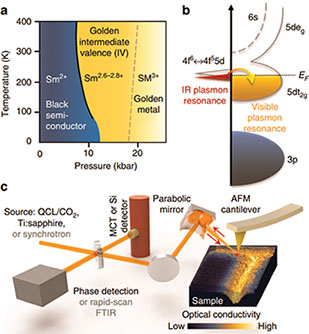
Near-Field Spectroscopic Investigation of Dual-Band Heavy Fermion Metamaterials

Broadband tunability is a central theme in contemporary nanophotonics and metamaterials research. Combining metamaterials with phase change media offers a promising approach to achieve such tunability, which requires a comprehensive investigation of the electromagnetic responses of novel materials at subwavelength scales. In this work, we demonstrate an innovative way to tailor band-selective electromagnetic responses at the surface of a heavy fermion compound, samarium sulfide (SmS). By utilizing the intrinsic, pressure sensitive, and multi-band electron responses of SmS, we create a proof-of-principle heavy fermion metamaterial, which is fabricated and characterized using scanning near-field microscopes with <50 nm spatial resolution. The optical responses at the infrared and visible frequency ranges can be selectively and separately tuned via modifying the occupation of the 4f and 5d band electrons. The unique pressure, doping, and temperature tunability demonstrated represents a paradigm shift for nanoscale metamaterial and metasurface design.
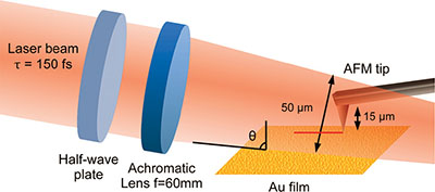
Subwavelength Nanostructuring of Gold Films by Apertureless Scanning Probe Lithography Assisted by a Femtosecond Fiber Laser Oscillator

Ignacio Falcón Casas, and Wolfgang Kautek
Nanomaterials 2018, 8(7), 536
https://doi.org/10.3390/nano8070536
Nanomaterials 2018, 8(7), 536
https://doi.org/10.3390/nano8070536
Optical methods in nanolithography have been traditionally limited by Abbe’s diffraction limit. One method able to overcome this barrier is apertureless scanning probe lithography assisted by laser. This technique has demonstrated surface nanostructuring below the diffraction limit. In this study, we demonstrate how a femtosecond Yb-doped fiber laser oscillator running at high repetition rate of 46 MHz and a pulse duration of 150 fs can serve as the laser source for near-field nanolithography. Subwavelength features were generated on the surface of gold films down to a linewidth of 10 nm. The near-field enhancement in this apertureless scanning probe lithography setup could be determined experimentally for the first time. Simulations were in good agreement with the experiments. This result supports near-field tip-enhancement as the major physical mechanisms responsible for the nanostructuring.
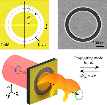
Spin-Symmetry-Selective Generation of Ultracompact Optical Vortices in Nanoapertures without Chirality

Tong Cui, Mingqian Zhang, Lin Sun, Shuyin Zhang, Jia Wang, Benfeng Bai, and Hong-Bo Sun
Small Struct. 2020, 2000008
https://doi.org/10.1002/sstr.202000008
Small Struct. 2020, 2000008
https://doi.org/10.1002/sstr.202000008
Nanoscale optical vortices (OVs) carrying orbital angular momenta can be generated via photonic spin–orbit interaction (SOI) in nanostructures and have important applications in many emerging fields such as quantum communication and optical manipulations. Existing OV generators such as metasurfaces and chiral structures suffer from discontinuous wavefront modulation, single-spin response, and bulk size. The photonic SOI in highly symmetric structures has been overlooked. Here, by studying the SOI in a plasmonic annular nanoaperture, a simple and reliable way for generating ultracompact OVs and OV array in nanoapertures without chirality is reported. The generation of a 3×3 OV array within a small area of 6×6 μm2 is demonstrated experimentally. Using a homemade spin-selective and phaseresolved near-field microscopic system, in the spin basis, the dynamic evolution of the wavefront of the generated OV is directly probed from the near-field to the far-field with subwavelength resolution, which intuitively reveals the SOI process.