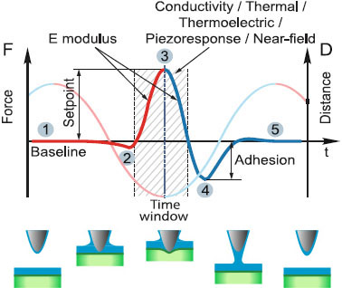
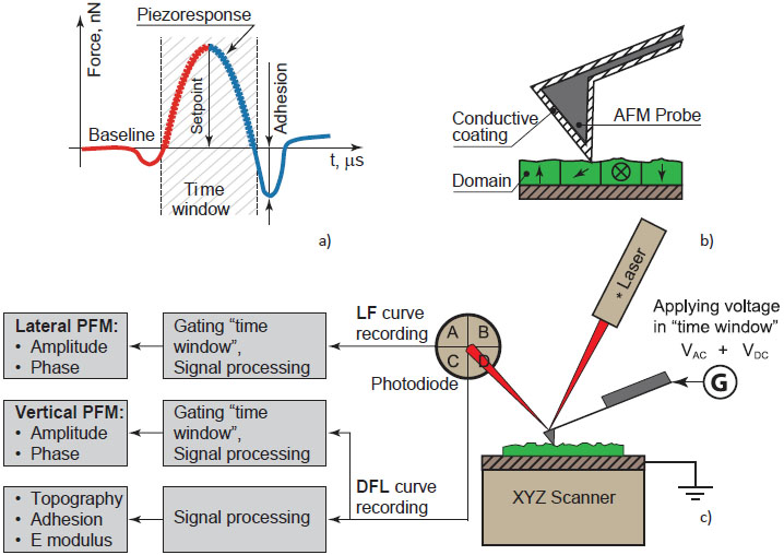
Other Applications
HD Conductive & Electrostatic Studies
Non-destructive Conductive studies simultaneously with QNM measurements
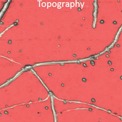
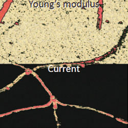
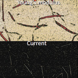
Electrical characterization of objects, that are weakly attached to the surface, has always been a challenge when using standard AFM modes like Conductive AFM. This was because often the tip moved or abraded the objects of interest. HybriD Mode drastically decreased the impact of lateral forces and simplified these experiments.
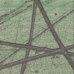
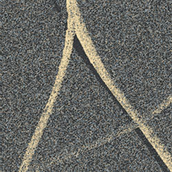
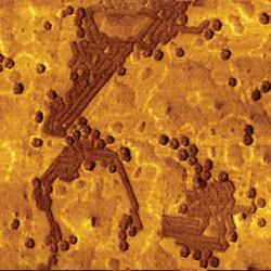
Comparison of conductive and mechanical maps shown in this example allows the clear identification of single nanotubes and bundles.
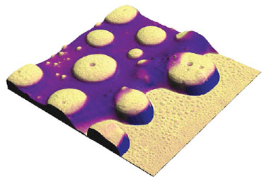
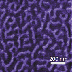
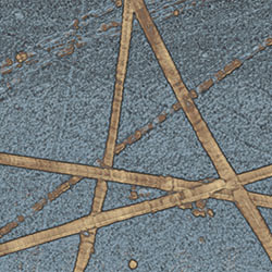
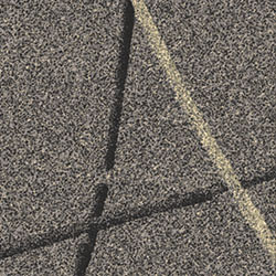
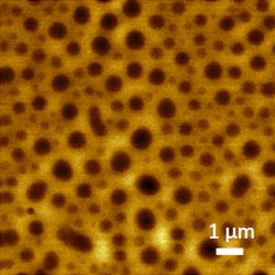
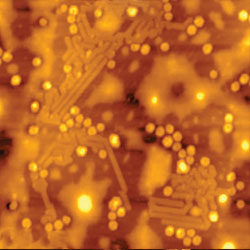
HD C-AFM study of carbon Nanotubes on Silicon. Sample courtesy: Dr. Kuljanishvili, Saint Louis University, Department of Physics. Scan size: 1×1 µm
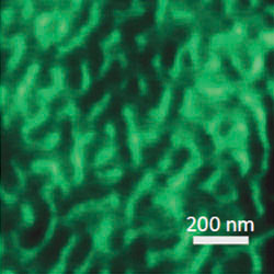
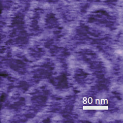
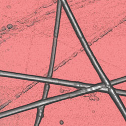
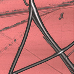
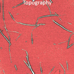
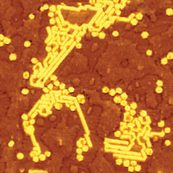
HD C-AFM study of coupled carbon and peptide nanotubes. Sample courtesy: Dr. J. Montenegro, University Santiago de Compostela. Scan size: 3×3 μm
Simultaneous electrostatic studies: HD KPFM, HD EFM and HD SCFM
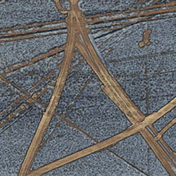
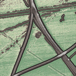
 HD KPFM study of WS2 monolayers grown on epitaxial graphene measured in vacuum. Topography is overlaid with surface potential. Sample Courtesy: Dr. Cristina Giusca, NPL, Prof. Mauricio Terrones, PSU. Scan size: 14×14 µm
New state-of-the-art HybriD 2.0 control electronics allows simultaneous resonant electrostatic studies using two-pass technique:
- Kelvin Probe Force Microscopy
- Electrostatic Force Microscopy
- Scanning Capacitance Force Microscopy
HD Scanning Thermoelectric Microscopy
Mapping of local Seebeck coefficient by HD Scanning Thermoelectric Microscopy
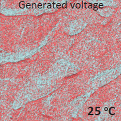
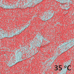
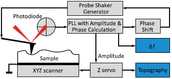
Thermoelectric studies of nanoscale structures like n-p junctions, conductive nanowires, graphene oxide etc. are currently of a great interest. HD Scanning Thermoelectric Microscopy (HD SThEM) allows non-destructive mapping of Seebeck coefficient with tip radius-limited spatial resolution. HD SThEM working principle is based on direct measurement of generated voltage when conductive tip and sample under different temperatures contact each other during fast force spectroscopy measurements.
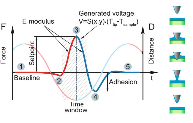
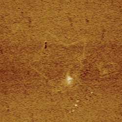
HD Scanning Thermoelectric Microscopy working principle,V – generated voltage, S(x,y) – Seebeck coefficient
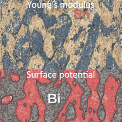
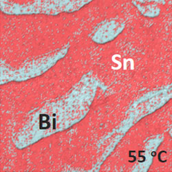
HD SThEM study of Tin-Bismuth alloy. Seebeck coefficient, S: Bi -72 mV/C, Sn -1.5 mV/C. Scan size: 7×7 µm
Bio HD & Vacuum HD Measurements
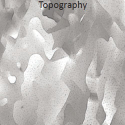
Bio HD: long-term liquid measurement combined with QNM
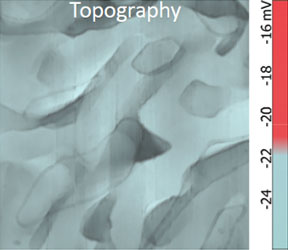
 Topography
 Young’s modulus
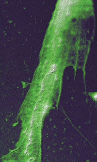
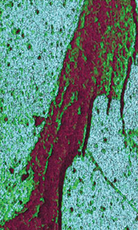
Bio HD study of Stem Cell fragment in Liquid. Elastic Modulus range: 0.2-1.5 kPa. Scan size: 18×30 µm
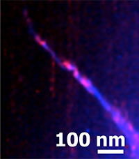
Tip Enhanced Raman Scattering (TERS, nano-Raman) is the technique for enhancement of weak Raman signals and for super-resolution Raman imaging with spatial resolution less than 10 nm.
As a result of comprehensive research performed together with NT-MDT SI customers and partners, we are now able to offer to AFM-Raman customers mass produced reproducible TERS probes.
TERS imaging requires prolonged tip-sample contact at each scanning point but Contact AFM is destructive for both the tip and the sample. Thereby, HD mode is a superior technique for cantilever-type TERS since it noticably increases the tip lifetime and makes possible TERS imaging of soft, loose and fragile samples.
Fast and artifact free studies with Vacuum HD
Vacuum measurements in amplitude modulation (AM) mode requires unacceptably low scanning speeds because of extremely high Q-factor of AFM probes. Being a non-resonant mode, HD mode allows at least 10 times faster imaging speed.
Another issue of AM mode in vacuum is that it is influenced by the electrostatic forces while the HD mode working principle allows automatic compensation of long-distance forces at each scanning point.
HD Scanning Thermal Microscopy
HD Scanning Thermal Microscopy working principle
 SThM probe
 Topography
 Temperature
 Temperature
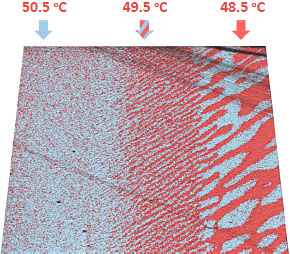
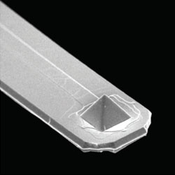
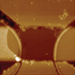
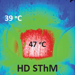
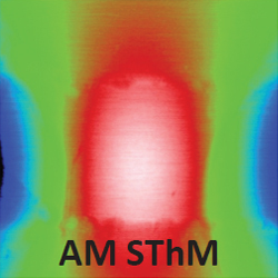
SEM image of AppNano VertiSense™ thermocouple probe and comparison of HD SThM and AM SThM techniques. Scan size: 17×17 µm
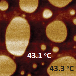
HD Scanning Thermal Microscopy (HD SThM) allows studying local thermal properties simultaneously with QNM measurements. From the hardware point of view it was implemented using AppNano VertiSense™ thermocouple probes. The thermal conductivity and temperature mapping modes (CMM, TMM) can be realized by positioning the AFM laser at the end or the central part of the probe, respectively. HD mode working principle allows exceptional spatial resolution of SThM measurements in comparison to conventional Amplitude Modulation (AM) mode. That was demonstrated in TMM of a micro-heater sample.
Simultaneous Thermal and QNM measurements
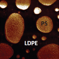
SThM and HybriD mode is the winning combination for distinguishing between the constituents of polymer blends as demonstrated in the example of a blend of polystyrene (PS) with low density polyethylene (LDPE) (see below). The difference in thermal conductivity of the polymers (PS – 0.12 W/mK; LDPE – 0.33 W/mK) allows the assignment of the colder matrix to LDPE and the hotter islands to PS.
 Topography
 Temperature
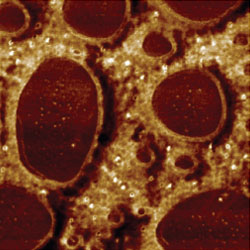 Adhesion
 Young’s modulus
HD SThM study of PS-LDPE. Scan size: 10×10 μm
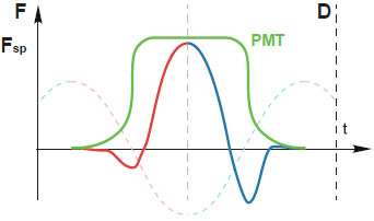
HD Phase-Locked Loop Studies
State-of-the-art HybriD 2.0 Control Electronics incorporates high-speed digital lock-in amplifiers (LIA) and phase locked loop detector (PLL) for advanced oscillatory resonance modes: Amplitude Modulation with Frequency Imaging (AM-FI) and Frequency Modulation (FM) modes. They provide exceptional level of spatial resolution of challenging flat and soft samples (self-assembled molecular structures etc.) thanks to ultra-precise control of the tip-sample interaction force. Additionally they allow mapping of its mechanical properties.
 Schematics of AM-FI mode
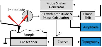 Schematics of FM mode
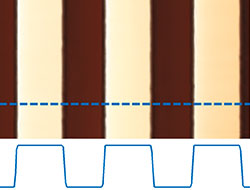
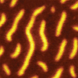
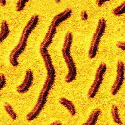
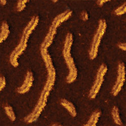
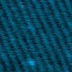
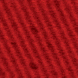
The two images below show topography and probe resonant frequency distribution over lamellar arrangement of short alkane C36H74 on graphite with a spacing of 4.5 nm. One can also see a couple of adsorbates formed on the lamellar surface by disordered alkane chains which are rarely observed by the traditional AM mode.
 Topography
 Frequency
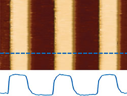
AM-FI mode images of C36H74 lamellae on graphite. Scan size 40×40 nm