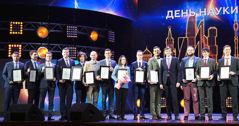
Moscow Government Award Goes to NT-MDT LLC Young Scientists
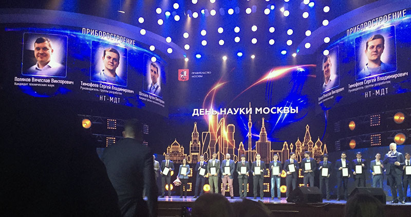
The Moscow Government Young Scientist award 2018, devoted to Russian Science Day, took place in the State Kremlin Palace on the 8th of February. The laureates were awarded by Moscow Mayor Sergey Sobyanin, President of the Russian Academy of Sciences Alexander Sergeev and Rector of the Lomonosov Moscow State University Viktor Sadovnichiy.
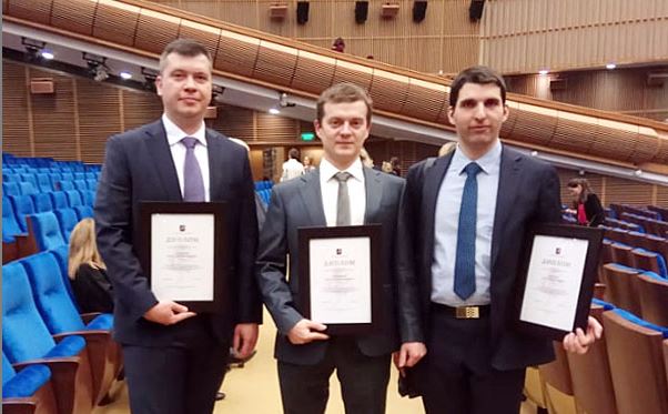
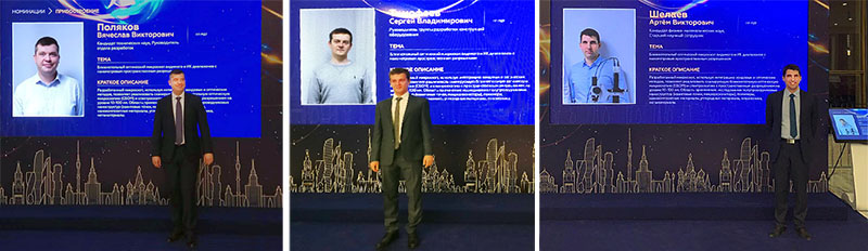
745 applications were filed in 2018 but only 77 nominees were awarded. The leading developers of NT-MDT LLC Dr. Polyakov Vyacheslav Viktorovich (PH.D.), Timofeev Sergey Vladimirovich (PH.D.) and Dr. Shelaev Artyom Viktorovich (PH.D.) were the prize winners in the Instrumentation Engineering category. The prize was awarded for the development of a scanning near-field optical microscope (SNOM) with a nanometer spatial resolution for the visible and IR ranges. The necessity to develop a new system for near-field microscopy and spectroscopy is determined by the growing interests of the industrial and scientific communities to combine measuring optical systems, which can allow a better spatial resolution beyond the diffraction limit in wider spectral ranges.
Our scientists developed NTEGRA Nano IR, a superior universal device, which combines atomic force microscopy (AFM) and near-field optical microscopy (SNOM) techniques in the visible and IR spectral ranges using various techniques for detecting the applicable signals. As a result, three Russian Federation patents were obtained based on the above mentioned research development. Another patent application is under consideration.
The developed NTEGRA Nano IR system is intended to define with nanometer resolution the composition and various physicochemical properties of heterogeneous samples such as semiconductor nanostructures, polymers, composite materials, carbon materials (nanotubes, graphene, nanodiamonds), proteins and to visualize localized radiation (light) in plasmonic structures, photonic crystals and metamaterials.
The system’s key features are:
- the capability to implement any geometry of excitation (top, bottom, side) and to record the optical response, for research of transparent and opaque samples based on a single platform;
- a record number of atomic force microscopy techniques, including non-resonant oscillation techniques;
- the ability to implement optical techniques associated with local signal amplification using AFM tips in the visible and near-IR ranges: Tip-enhanced giant Raman Scattering (TERS), Tip-enhanced Fluorescence Spectroscopy (TEFS), etc., which ensures the achievement of nanometer-based spatial resolution;
- the ability to work with aperture sensor probes with configurations for clearance, collection and reflection, which allows the use of SNOM techniques to investigate samples with a spatial resolution of approximately 100 nm;
- implementation of scattering SNOM mode in the visible and mid-IR ranges. Providing microscopic and spectroscopic measurements with a spatial resolution of 10 nm, which is more than two orders of magnitude larger than the diffraction limit for the corresponding optical range.
It is especially necessary to note the inclusion of the intelligent software module ScanT™. With its implementation, the application of basic AFM amplitude modulation (semi-contact) techniques are greatly facilitated.
The ScanT™ module allows you automatically receive artefact-free images with a minimized noise level.
Automatic adjustment of scanning parameters and image processing are carried out using neural networks ideology. With a minimal knowledge of sample properties, ScanT™ is equally useful for beginners as well as for experienced users, ensuring high-quality and reliable results.