


1.3.3 Measurements of the Electronic States Density
In chapter 1.3.1 we considered the spectroscopy of electronic states. Meanwhile, at given
 it is possible to measure the electronic states distribution across the sample surface.
The electronic states density distribution measurement is performed in parallel with surface topography imaging in the
 mode. Instead of constant tip bias
 , the alternating voltage
 is applied between sample and tip, where
 – the alternating signal having amplitude
 (Fig. 1). Then, the net tunneling current is proportional to the following
 ,
,
(1)
where
 and
and
 .
.
 ,
,
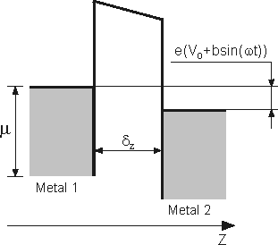
Fig. 1. Diagram of MIM system, when applied voltage is modulated as
.
Thus, the total current flowing through the tunneling gap is equal to
 , where
 – alternating component. Because
 is held constant during the scan and
 , the alternating tunneling current amplitude is proportional to the electronic states density
 . Hence, measuring the alternating current amplitude during scan allows for the mapping of the electronic states density in standard units. Since
,
. Hence, measuring the alternating current amplitude during scan allows for the mapping of the electronic states density in standard units. Since
,
 then is actually
 .
.
The frequency
 , as mentioned above, should be much more than the reciprocal feedback integrator time constant and be limited by maximum permissible scan frequency.
Summary.
- Modulation of applied voltage
 results in oscillations of tunneling current
 . Amplitude of such oscillations depends on electron properties of electrodes, which create a tunneling contact.
 - Using this method, it is possible to measure distribution of electron state density on investigated sample surface.
References.
- G. Binnig, H. Rohrer. Helv. Phys. Acta. – 1982, – V. 55 726.
- A. Burshtein, S. Lundquist. Tunneling phenomena in solid bodies. Mir, 1973 (in Russian).
- E. Wolf. Electron tunneling spectroscopy principles. Kiev: "Naukova Dumka", 1990, 454 p. (in Russian).