MDT-file: Download
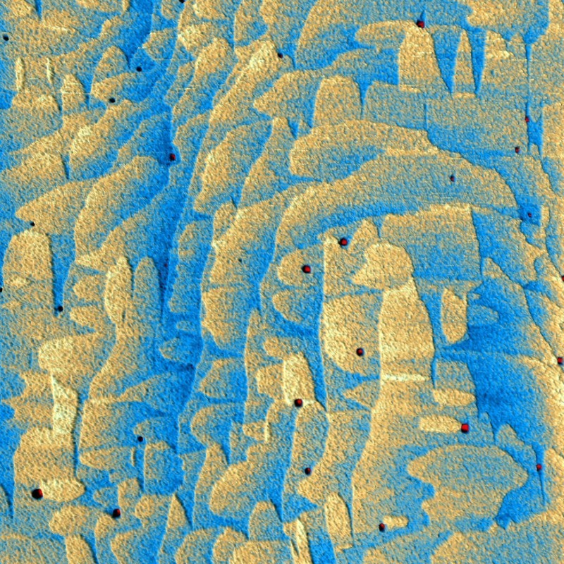
Monolayer steps, 0.14 nm high, on the Si (001) surface after growing a very thin homoepitaxial surface at room temperature. Surface pits arise from impurity effects. Semi-contact image.
Image and sample courtesy of Dr. Jerry Floro, University of Virginia, USA


+1-480-493-0093