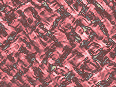
Semiconductor layer InGaAs 47 nm thickness. Layer is grown by Atomic Layer MBE on GaAs substrate at 500 ℃.
Image courtesy of Eremenko V., IMT RAS, Russia.
Sample courtesy of Dr. Luisa Gonzalez, Institute of Microelectronics CSIC, Madrid, Spain.


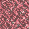
Semiconductor layer InGaAs 47 nm thickness. Layer is grown by Atomic Layer MBE on GaAs substrate at 500 ℃.
Image courtesy of Eremenko V., IMT RAS, Russia.
Sample courtesy of Dr. Luisa Gonzalez, Institute of Microelectronics CSIC, Madrid, Spain.