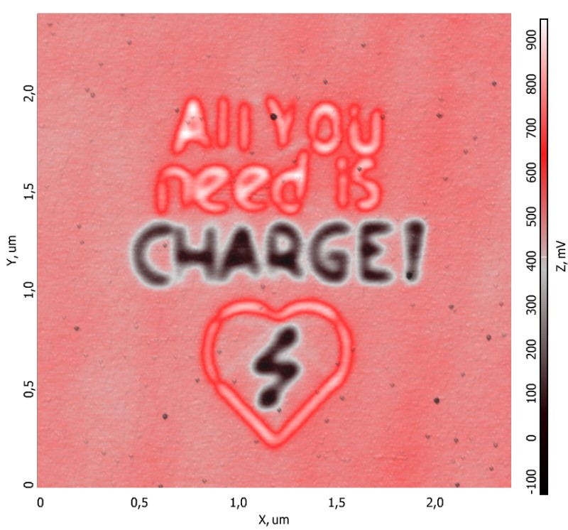
Image shows the distribution of the surface charge induced under the layer of Silicon Oxide using voltage nanolithograpy overlaid over the surface topography. Black color correspond to -100 mV, white color - to +900 mV. Lithography was done by HA_HR/W2C conductive #probe in contact mode. Voltage applied within the range of -3..+3 V. Imaging was done in two-pass AM-KPFM mode.
Device: NEXT
Tip: HA_HR/W2C
Image Courtesy: Dr. Stanislav Leesment


+1-480-493-0093