Application Note 100 (pdf 2.8 Mb)
- Enhancement factors: 100x and more
- Lateral resolution in TERS: down to 10 nm
- High speed TERS mapping
- Based on commercial AFM cantilevers (contact, non-contact): multiple AFM modes, excellent imaging performance
The resolution of “classical” optical imaging is limited by diffraction. Light cannot be focused by conventional refractive or reflection optics into a spot smaller than half of the wavelength (about 200 nm for visible light). This fact has impacted on the size limit of light microscopy and spectroscopy for the last few centuries. Currently, new optical microscopy techniques are being developed that break the Abbe diffraction limit and give the capability to resolve features substantially smaller than 100 nm by using visible light.
HIGH RESOLUTION OPTICAL IMAGING BY TIP-ASSISTED TECHNIQUES
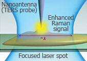
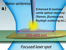
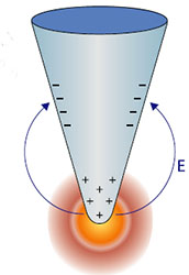
One of the promising approaches that break the optical diffraction limit is the so-called “apertureless” or “tip assisted” technique. A nano-antenna (a specially prepared AFM probe) is excited by a tightly focused excitation laser spot (Fig. 1 (a)), placed at the apex or, depending on the nano-antenna working principle, at some other part of the nano-antenna. Under specific conditions, the nano-antenna can localize and enhance the excitation electromagnetic field and/or sample optical response in very close proximity to the tip apex.
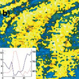
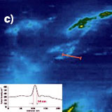
Fig. 1. (a) Principle of Tip-Enhanced Raman Scattering (TERS) and other tip-assisted optical techniques. (b Nano-Raman (TERS) map of carbon nanotube; overlay of G-band (blue) and D-band (red). Spatial resolution of the TERS map is ~10 nm. (c) Nano-Raman (TERS) map of thin molecular film on Au substrate. Spatial resolution of the TERS map is <15 nm
The nano-antenna apex effectively works as a localized “nano-emitter” or “nano-scatterer” of light. When scanning the sample with respect to this nano-antenna, the obtained map of sample optical response (Raman and Rayleigh scattering, fluorescence, etc.) has a lateral resolution which is determined not by the laser spot size but by the size of the electromagnetic field localization at the nano antenna apex. Theoretically, the resolution of these tip-assisted techniques can reach size scales of less than 10 nm, leading to true nanoscale optical imaging.
One of the most common types of tip-assisted optical imaging techniques is Tip-Enhanced Raman Scattering (TERS or “nano-Raman”) which is when a nano antenna is used to locally enhance the Raman scattering signal from a sample.
Raman maps with nanometer scale resolution provide a route for chemical identification on the nanometer scale. Fig. 1 (b), (c) show examples of “nano-Raman” maps of various objects with a resolution of ~12-15 nm which is close to the theoretical limit. There are also other tip-assisted techniques for high resolution optical microscopy: Tip Enhanced Fluorescence Microscopy, TEFM (when a sample’s fluorescence signal is enhanced), scattering near-field optical microscopy, s-SNOM (when light elastically scattered
by a nano-antenna is measured) and others.
In the remainder of this paper we will mainly use the “TERS” acronym to describe the experiments, instrumentation and measurements procedures since TERS experiments are the most widely used. TEFM and s‑SNOM experiments are essentially the same as TERS from hardware point of view. They only differ in the types of probes used, and the optical signal measured.
NANO-ANTENNAS FOR TERS AND OTHER TIP-ASSISTED OPTICAL TECHNIQUES
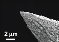
The most commonly used type of nano-antenna for nano-scale optical imaging is a sharp metal tip (usually gold or silver) which has a localized surface plasmon at the very end (Fig. 2 (a)) having a frequency close to that of the excitation laser light. The power density of the light can be locally increased by many orders of magnitude in the area within ~10 nm of the tip end. Tips are usually either etched from a metal wire (Fig. 2 (b)) or metal is deposited onto a standard AFM cantilever. Several,
more elaborate probes are also used as nano-antennas: metal tips with bow-tie structures at the end, tips with special periodic structures for effective excitation and focusing of surface plasmon polaritons as well as others.
 a)
a)
 b)
b)
Fig. 2. (a) Electron charge density oscillations of a localized surface plasmon at the end of a sharp metal wire; corresponding distribution of the electromagnetic field (light) localized a few dozen nanometers around the tip apex. (b) Experimental example of a TERS probe (etched metal wire). Data from S. Kharintsev, A. Noskov, G. G. Hoffmann and J. Loos, Nanotechnology 22 (2011), 025202
PRINCIPLES BEHIND A SUCCESSFUL TERS EXPERIMENT
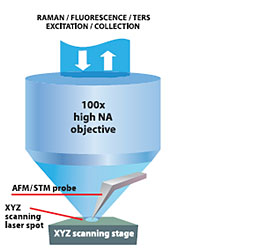
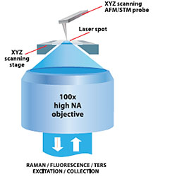
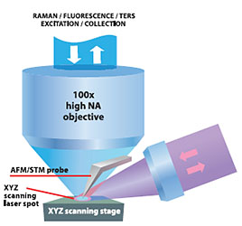
In order to study the interaction between light and an AFM probe (nano-antenna), the following strict requirements are necessary for the instrumentation: Integration of the AFM with high resolution objective lenses in different configurations (Fig. 3) Illumination and signal collection from the top, from the bottom and from the side is required for different experiments and different sample types. A high resolution (high numerical aperture - NA) objective lens is the key factor for the successful measurement of TERS signals. It maximizes light collection efficiency and, at the same time, minimizes collateral excitation and collection of the non-enhanced optical signal coming from the sample.
Fig. 3. Various geometries for TERS and other tip-assisted optical experiments: Illumination/collection from the top, from the bottom and from the side Dual Scan: sample scanning AND laser spot scanning relative to AFM probe.
For successful TERS mapping not only should the sample be scanned with nanometer precision but also the AFM probe must be positioned automatically inside the laser spot with the precision of a few tens of nm. To accomplish this task, the tightly focused laser spot or the tip should be automatically scanned with respect to one another in the X, Y and Z directions with nm accuracy and repeatability.
Ability to support different AFM probes: AFM cantilevers, STM tips, different etched wires,etc.
There are many different types of nano-antennas. In order to be able to work with all of them, the instrument must support numerous types of AFM probes (cantilevers,wires,fibers,etc.) and all types of feedback mechanisms (laser feedback, tuning fork feedback, tunnelling current feedback etc.).
Mechanical stability.
In order to detect the near-field effects that produce high resolution optical maps, a nano-antenna has to be positioned a few nm from the sample and its proximity maintained with very high stability without damaging the sensitive TERS tip. This dictates requirements for precision, speed and sensitivity of the AFM feedback electronics and mechanical stability of the system. Mechanical and temporal stability is also crucial in keeping the nanoantenna precisely inside a tightly focused laser spot for long-term experiments.
Integration with a dedicated Raman spectrometer.
The key requirements for a well integrated Raman system for a TERS experiment are: properly expanded and collimated excitation laser beam to achieve the minimum laser spot size on the sample, high confocality for minimizing “background” (non-enhanced) signal detected from the sample, fast automated changing of the excitation lasers and automated polarization rotation for optimizing the resonant excitation of surface plasmons in the nano-antenna, high sensitivity and imaging speed.
Seamless software and hardware Integration of AFM and optical spectroscopy techniques.
Unified and comprehensive control software is required to run a complicated TERS experiment combining all of the AFM and spectroscopy hardware capabilities. All Raman and AFM components of the instrument should be easily controlled from the same program. The software should not be a limiting factor for the TERS scanning speed- all delays when communicating with scanners and optical detectors should be minimized. AFM, Raman and TERS images should be collected and analysed in one seamless software program.
All of the above requirements are successfully incorporated in the NTEGRA Spectra AFM-Raman-SNOM-TERS Instrument. TERS data obtained with the NTEGRA Spectra is shown on next page.
GRAPHENE VISUALIZED BY TERS
Using a Silver STM tip as a TERS probe
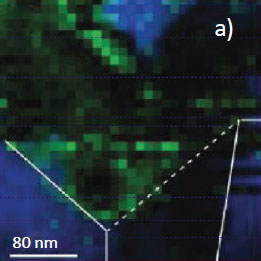
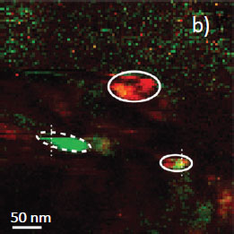
Fig. 4 (a) shows a TERS image of graphene (produced by standard CVD on a copper substrate) obtained by using etched silver STM tip as a TERS probe. The experiment is done in the so-called “gap-mode”: when both tip and substrate are metallic and tunnelling current feedback is used. The green colour represents intensity of the graphene 2D band - corresponding to pristine graphene areas. The blue colour shows intensity in the 2800‑3000 cm-1 region (typical for CH stretching modes) - corresponding to areas with CH-terminated graphene. It is notable that CH stretching bands are not seen at all in conventional confocal Raman images - due to their very low intensity. A TERS image of graphene produced by the Scotch-tape method and deposited onto a gold substrate is shown on Fig. 4 (b). Two defect areas inside the single graphene layer are identified on the image by the intensity of D-band (red areas, arked by solid line circles). The dimensions of the defect areas are 75x45 nm and 55x25 nm respectively. Precise analysis
of line cross-sections taken from the above Raman maps shows that all the TERS images were recorded with a lateral resolution of less than 12 nm.
Fig. 4. (a) TERS maps of single layer CVD Graphene on copper substrate. Green color: areas of pristine graphene (2D band intensity). Blue color: CH-terminated graphene areas (CHbands intensity). (b) TERS map of mechanically exfoliated single layer graphene on Au substrate. Green color: 2D band intensity. Red color: Dband intensity (areas with strong defects). Resolution of all Raman maps is <12 nm. J. Stadler, T. Schmid, and R. Zenobi, Nano Letters (2010), 10, 4514-4520
Using a Gold Coated Cantilever.
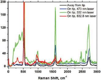
Fig. 5 shows TERS data on multi-layer graphene (on Si/SiO2 substrate) using an Au-coated cantilever as a TERS probe. The TERS enhancement takes place only when the localized surface plasmon at the tip has energy close to that of the excitation laser photons. This is clearly demonstrated in Fig. 5 (a) showing experimental wavelength dependance of the enhancement. TERS spectra are given for red, green and blue excitation lasers and compared to conventional confocal Raman spectrum taken away from the TERS probe. The TERS enhancement factor reaches its maximum with the green laser.
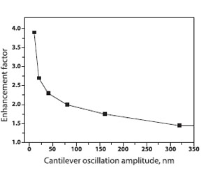
Fig. 5. (a) Confocal Raman and TERS spectra of a few-layer graphene taken using different excitation lasers with the same TERS tip. TERS enhancment factor strongly depends on the laser wavelength due to surface plasmon resonance. (b) TERS enhancement factor as a function of cantilever oscillation amplitude demonstrating near-field nature of the enhancement. (c) TERS map of graphene edge (G-band intensity). Data from A. Schokin (NT‑MDT SI)
Fig. 5 (b) shows TERS enhancement factor as a function of cantilever oscillation amplitude. It rapidly increases for cantilever amplitudes smaller than 50 nm, demonstrating the spatial localization of the TERS enhancement effect. The TERS map (intensity of the G-band) of the graphene edge area is given in Fig. 5 (c), showing the lateral resolution is much higher than conventional confocal Raman microscopy.
SEMICONDUCTOR STRUCTURES VISUALIZED BY TERS
Imaging and Strain Analysis of Nano-scale SiGe Semiconductor Structures The periodic SiGe line structure, Fig. 6 (a), is used as a test sample for TERS imaging of nanoscale Si devices - to study chemical composition and crystal lattice stress. The line structure has an average period of 95 nm - comparable to the dimensions encountered in presently available CMOS devices.
Simultaneously measured AFM and TERS maps are shown in Fig. 6 (c), (d), (e). The periodic line structure is clearly resolved in the Raman images, indicating the lateral resolution of the Raman maps. As seen in the line profile, the intensity of the Raman signal from the SiGe layer, (Fig. 6 (e)), increases sharply at the position of each SiGe line due the higher SiGe thickness (40 nm) compared to 10 nm thickness between the lines. Conversely, the Raman signal from the Si substrate is diminished at the positions of each SiGe line. Because the enhancing TERS tip in these areas is far away (>50 nm) from the substrate the TERS enhancement form the Si disappears.
Fig. 6 (b) compares Raman spectra taken from the individual SiGe lines and from the area of a thin, 10 nm, SiGe layer away from the line structure. Raman band positions are used to calculate stress
(σxx = σyy = σ0 = -1.53 GPa) within the remnant 10 nm thick SiGe layer away from the line pattern. The patterning process leads to strong stress relaxation within the freestanding SiGe lines. From the spectra acquired from the TERS measurements, a stress value of approximately σxx = -190 MPa is calculated, corresponding to a stress relaxation of about 88% compared to the initial value before pattering.
The relaxation of the compressive stress in the substrate below the lines as shown in Fig. 6 (b). This small amount of tensile stress could be the reason for the observed slight special shift of the Si substrate peak to lower wavenumbers as compared to the stress-free peak position. The results demonstrate the capability of the TERS technique to characterize the stress in Si based nanostructures with <50 nm spatial resolution - as required for the investigation of current leading edge CMOS devices.
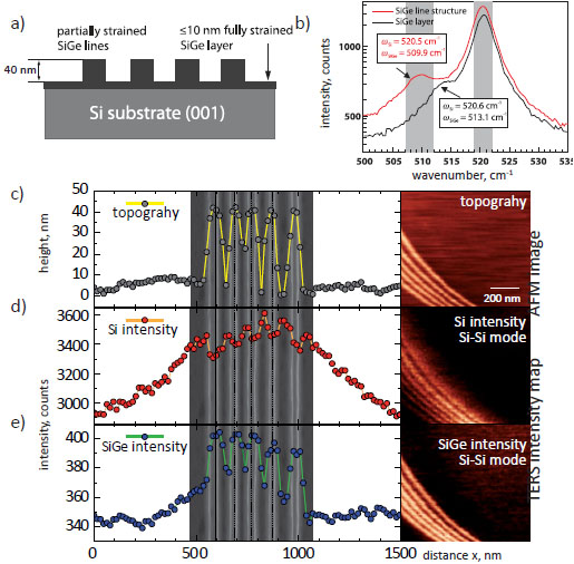
Fig. 6. (a) Periodic SiGe line structure on Si substrate. (b) Comparison of TERS spectra from a SiGe line (red) and the remnant thin SiGe area a few μm away from the line structure. Peak positions of SiGe band are different indicating different stress states. (c) AFM topography and (d), (e) simultaneously measured TERS maps of Si-Si phonon band in Si and in SiGe material correspondingly; right panels show 2D maps (2x2 μm), left panels show corresponding line crosssection (from the lowest scan line). Resolution of Raman maps is <50 nm. Data from P. Hermann, M. Hecker, D. Chumakov, M. Weisheit, J. Rinderknecht, A. Shelaev, L. M. Eng, Ultramicroscopy 111(2011) 1630-1635.
CARBON NANOTUBES VISUALIZED BY TERS
Au coated AFM cantilever as a TERS probe.
Conventional micro-Raman and TERS mapping of single-walled carbon nanotubes is shown in Fig. 7. Nanotubes were deposited from solution onto a microscope cover glass substrate. Experiments were done in the inverted geometry (illumination from bottom) using a 633 nm excitation laser and an Au coated cantilever as the TERS probe.
The Confocal Raman map of the sample (Fig. 7 (a)) has a diffraction limited resolution of 250 nm. Details of nanotube bundles are not revealed in the image.
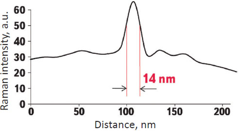
The TERS image in Fig. 7 (b), (c) gives a lateral resolution of ~14 nm and provides detailed information about the structure of the nanotube aggregates.
A complete Raman spectrum was recorded at every pixel of the TERS map (100x100 pixel image ). Detailed analysis of different Raman bands on the obtained TERS map allowed differentiating nanotubes of different types (metallic or semiconducting), different diameters, as well as detecting nanosize amorphous carbon contaminants with a resolution close to 10 nm.
Fig. 7. (a) Conventional micro-Raman and (b) Tip-Enhanced Raman maps of nanotube bundle aggregate (G-band intensity). Line cross-section taken from (b) showing lateral resolution of TERS imaging ~14 nm. Data from Andrew Chan and Sergey Kazarian, Nanotechnology 21 (2010) 445704
 a)
a)
 b)
b)
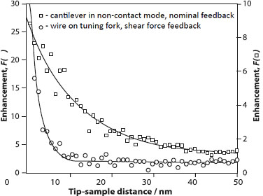
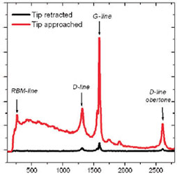
Fig. 8. (a) TERS (nano-Raman) map of individual single-walled nanotube bundle. Lateral resolution is <50 nm. (b) Raman spectra from the bundle with (red) and without (black) enhancing TERS probe. (c) TERS enhancement factor vs. Tip-sample distance for vertically oscillating AFM cantilever and horizontally oscillating Au wire. S. Kharinstev, G.G. Hoffmann, G.de With and J.Loos Nanotechnology 18 (2007), 315502
Etched Au wire as TERS probe.
The TERS image of an individual single walled nanotube bundle measured with an etched metal wire as the TERS probe is shown in Fig. 8 and resolution of 50 nm is demonstrated in Fig. 8 (c) shows the tip approach curves (TERS enhancement factor as a function of tip sample distance) for two types of TERS probes: horizontally oscillating metal wire attached to the tuning fork (oscillation amplitude < 10 nm) and vertically oscillating AFM cantilever (oscillation amplitude ~40 nm).
The data for the tuning fork demonstrated that the TERS effect is localized to approximately 10 nm near the tip. The approach curve for the AFM cantilever is less steep due to the large amplitude of vertical oscillation. Even though the average distance from the cantilever tip to the sample is large (~30 nm), during part of the oscillation cycle the tip is only a few nm from the sample, producing a visible enhancement. Measurements were performed in the inverted AFM-Raman geometry.
POLYMERS VISUALIZED BY TERS
Phase separation studies of polymer blend film.
Phase separation behaviour of a partially miscible PMMA/SAN (70/30 wt %) thin polymer film was studied by TERS mapping. Regular confocal Raman and TERS spectra from the film are compared on Fig. 9 (a). The spectra were recorded at the same acquisition time. The net enhancement factor of Raman signal is ~15x that corresponds to ~1500x enhancement area (~20x20 nm). Such TERS enhancement allows mapping with much higher speed and lateral resolution compared to conventional confocal mapping. TERS maps of the SAN Raman band for the thin film after 2 min annealing at 250 °C are shown in Fig. 9 (b), (c).
No sharp phase boundary is observed on Fig. 9 (c) indicating an early stage of the phase separation for the given annealing conditions. Meanwhile, films treated for 5 min at 250 °C showed completely different phase separation behaviour with larger SAN domains and sharper phase boundaries.
 a)
a)
 b)
b)
Fig. 9. (a) Regular confocal Raman and TERS spectra of SANPMMA thin polymer lend film. (b), (c) High resolution TERS maps of SAN Raman band, showing SAN component distribution in the the blend. Data from L. Xue, W. Li, G.G. Hoffmann, J.G.P.Goossens, J.Loos and G.de With, Macromolecules (2011)
ORGANIC SAMPLES VISUALIZED BY TERS
High resolution TERS aping of thin organic films on Au substrate.
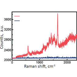
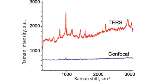
Fig. 10 (a) compares confocal Raman and TERS spectra of a thin nile blue film (NB)/brilliant cresyl blue (BCB) layer on a gold substrate. An etched sliver tip is used in STM feedback regime with gap-mode geometry. The conventional confocal Raman signal from the layer is almost absent, while the TERS spectrum shows strong Raman bands specific to the NB and BCB molecules.
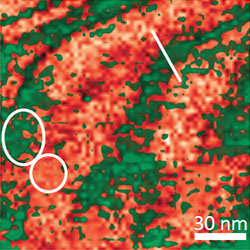
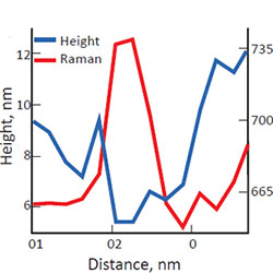
Fig. 10. (a) Confocal Raman and TERS spectra from a thin film of Nile Blue and CB dye molecules on Au surface. (b) Overlay of the STM topography (orange color) and TERS map of nile blue marker Raman band (green color) showing nonuniform distribution of the molecules on the surface. (c) Height and Raman (TERS) profiles along the line cut indicated on the image (b). The lateral resolution of the TERS map is <14 nm. (c) J.Stadler, T.Schmid,and R.Zenobi, Nano letters (2010) 4514-4520
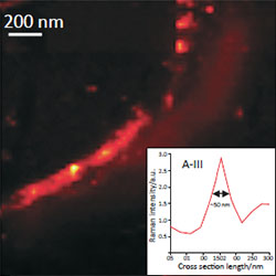
The TERS enhancement factor is estimated to be at least 107 - enough for single molecular sensitivity in Raman imaging. The overlay of the STM and TERS (NB band intensity) images shown on Fig. 10 (b) demonstrates non-uniform distribution of the molecules on the substrate. In some areas the density of NB molecules is correlated with the topography of the surface, in other areas (example shown by circles), nonuniform distribution of molecules is observed on the completely flat areas of the substrate. The selected line profile of Raman intensity from the TERS map Fig. 10 (c) shows the resolution of Raman imaging to be at least 14 nm.
PATTERNED THIOL MONOLAYERS VISUALIZED BY TERS
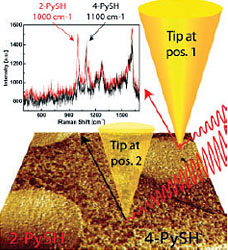
Distribution of two isomeric thiols (2-mercaptopyridine (2-PySH) and 4-mercaptopyridine (4-PySH)) in a self-assembled monolayer (SAM) on a gold surface was measured by STM‑TERS (Fig.11). The circle pattern of the 2-PySH thiol SAM was produced by micro-contact printing. SAMs of such thiols are used as protective layers on metal surfaces, act as a basis for (bio-)sensors, and have been proposed as components for molecular electronics. The large signal enhancement of TERS was employed here to detect monolayer coverage of weakly scattering analytes that are not detectable with normal Raman spectroscopy. This emphasizes the usefulness of TERS for studies of organic samples that are not feasible by conventional Raman spectroscopy.
Fig. 11. TERS spectroscopy of a selfassembled thiol monolayer on a gold surface. Pronounced Raman spectra from mono/ayers of 2-PySH and of 4-PySH are detected when TERS probe is used for local enhancement. TERS images of a patterned monolayer of two isomeric thiols based on the intensity of marker bands of (a) 2-PySH, (b) 4-PySH,and (c) the ratio of both. J.Stadler, I Schmid, L. Opi/ik, P. Kuhn, P. S. Dittrich, and R. Zenobi, Beilstein J.Nanotechnology, (2011) 2:509-515
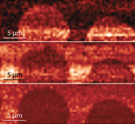
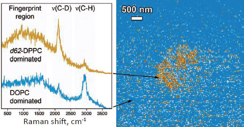
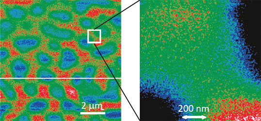
LIPID MONOLAYER VISUALIZED BY TERS
Fig. 12. STM-TERS allowed the direct measurement of the lipid distribution in a mixed supported lipid monolayer in a full-spectral map with high spatial resolution. The image is based on the intensity ratio of the C-D stretch mode (related to deuterated DPPC) and the C-H stretch mode (related to DOPC), and reveals an approx. 1-μm large domain that is dominated by DPPC. Supported lipid layers are model systems to gain insight into the processes associated with the compartmentalization of cell membranes into socalled lipid rafts.